Large-bandgap host materials for phosphorescent emitters
a phosphorescent emitter and host material technology, applied in the direction of discharge tube luminescnet screen, discharge tube/lamp details, organic chemistry, etc., can solve the problems of significant phosphorescence quenching, reduced efficiency, and lower triplet energy sta
- Summary
- Abstract
- Description
- Claims
- Application Information
AI Technical Summary
Benefits of technology
Problems solved by technology
Method used
Image
Examples
example 1
Synthesis and Characterization of Representative Compounds of the Invention
Conjugated Polymers of the Invention Having Meta-Linkage
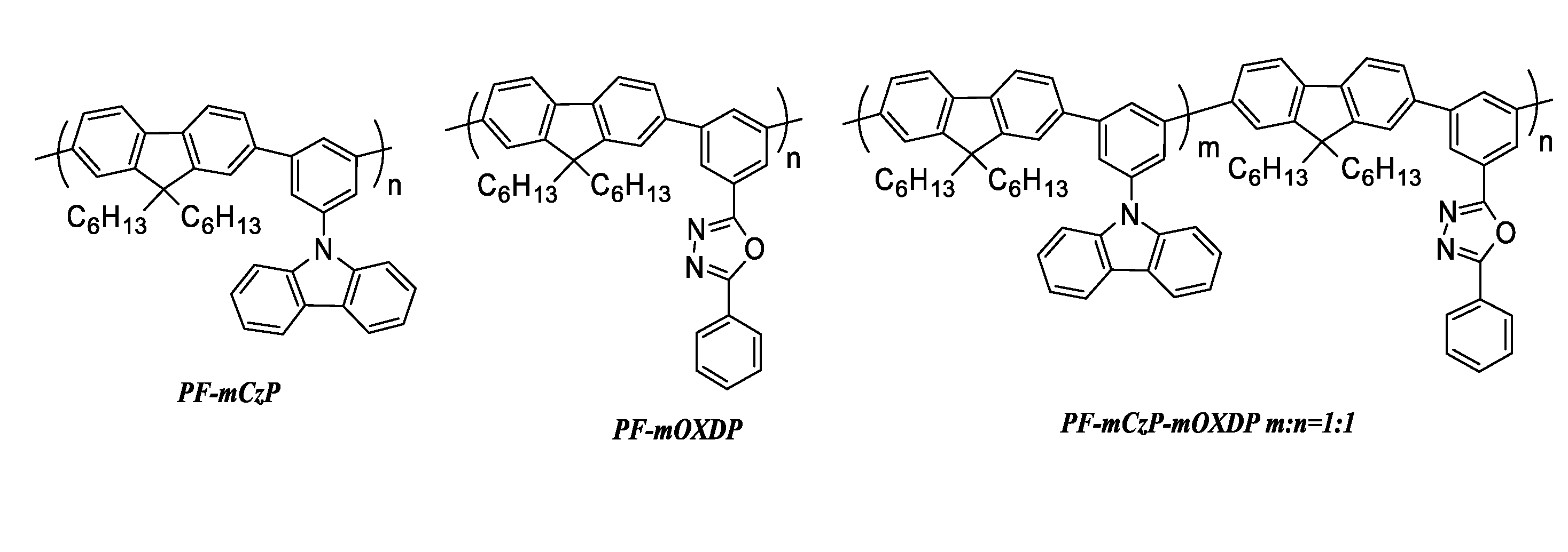
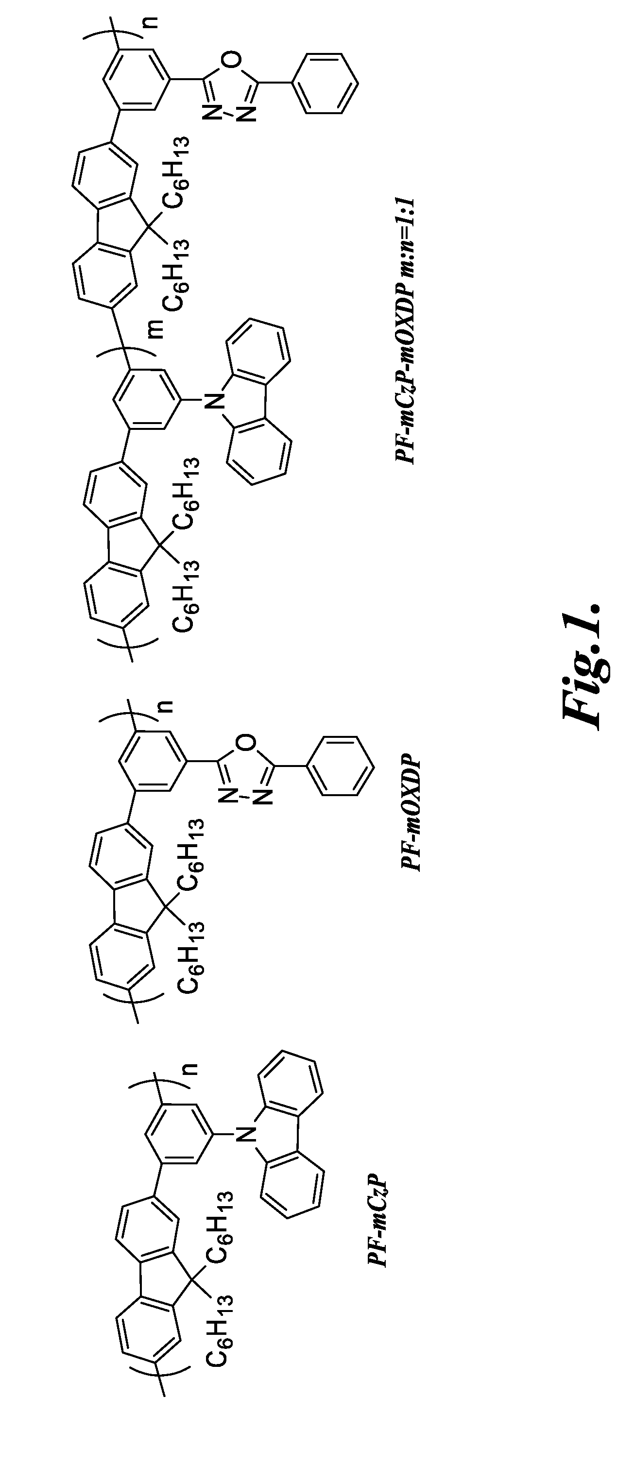
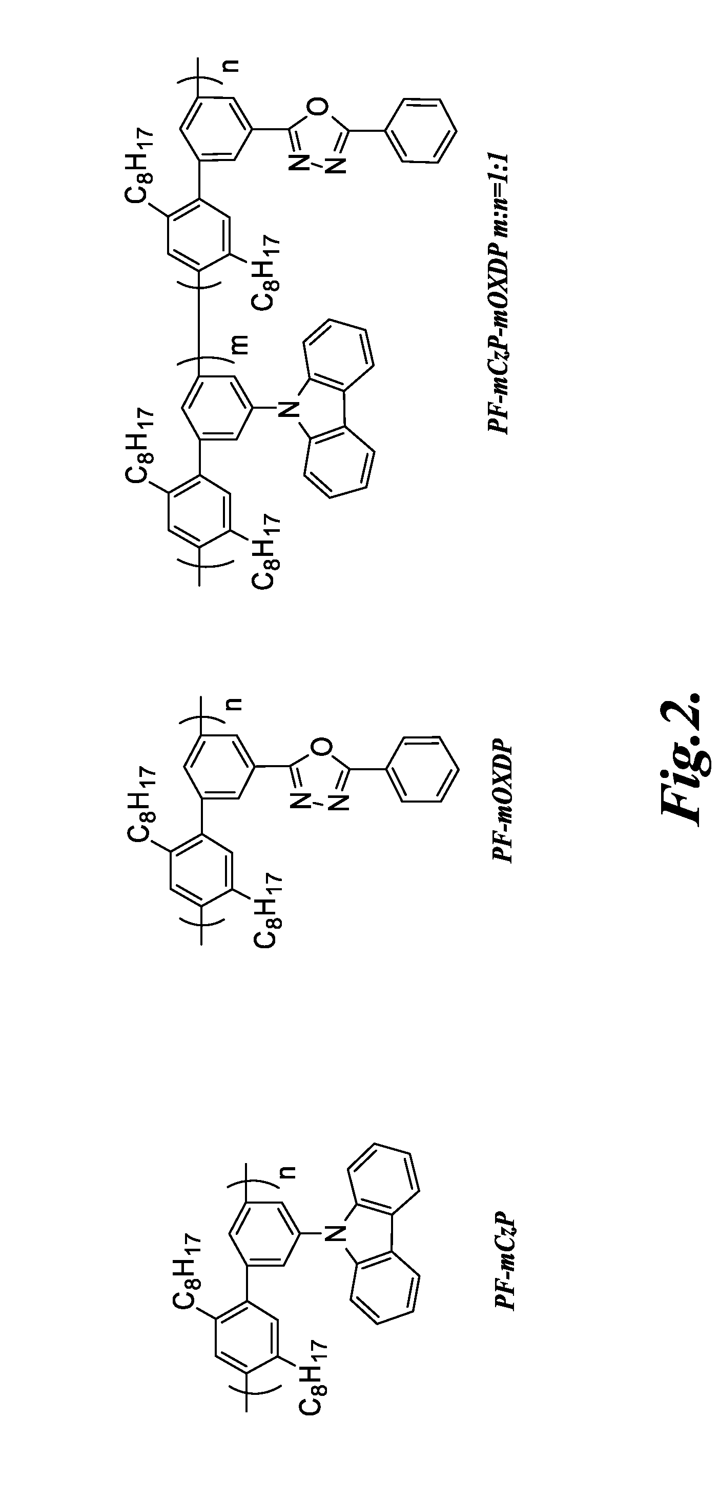
[0088]The structures of PF-mCzP, PF-mOXDP and PF-mCzP-mOXDP are illustrated in FIG. 1. The structures of PP-mCzp, PP-mOXDP, and PP-mCzp-mOXDP are illustrated in FIG. 2. The alternating copolymers PF-mCzP and PF-mOXDP were synthesized by the Suzuki coupling reaction between fluorene diboronate and 9-(3,5-dibromophenyl)-9H-carbazole, 2-(3,5-dibromophenyl)-5-phenyl-1,3,4-oxadiazole, respectively. A bipolar, random copolymer, PF-mCzP-mOXDP containing both the electron-transporting oxadiazole- and the hole-transporting carbazole-phenylene was also synthesized for balanced charge injection and transport. The structures of the polymers were confirmed by 1H NMR.
[0089]All synthesized polymers are readily soluble in common organic solvents, including toluene, chloroform, and THF. The molecular weight of the synthesized polymers was determined by gel permeation chr...
example 2
Light-Emitting Device Fabrication and Characterization
[0109]Light-emitting devices of the present invention are illustrated in FIGS. 11 and 12. FIG. 11 illustrates the most basic device structure of the invention. The device incorporates a film made of the compounds of the invention intermediate two electrodes. A more complex device structure can incorporate hole-transport layers, electron-transport layers, hole and electron-blocking layers, and charge-injection-enhancing layers adjacent to the electrodes. A typical complex device of the invention is illustrated in FIG. 12. Devices were fabricated on indium tin oxide (ITO)-coated glass substrates. The substrates were ultrasonicated sequentially in detergent, deionized water, 2-propanol, and acetone and were treated with O2 plasma for 10 min before use. A layer of thermally-crosslinkable precursor, PS-TPD-TFV, in 1,2-dichloroethane with the concentration of 5 mg / mL was spin-coated onto the ITO and was thermally cross-linked at 235° C...
PUM
| Property | Measurement | Unit |
|---|---|---|
| Wavelength | aaaaa | aaaaa |
| Wavelength | aaaaa | aaaaa |
| Energy | aaaaa | aaaaa |
Abstract
Description
Claims
Application Information
 - R&D
- Intellectual Property
- Life Sciences
- Materials
- Tech Scout
- Unparalleled Data Quality
- Higher Quality Content
- 60% Fewer Hallucinations
Browse by: Latest US Patents, China's latest patents, Technical Efficacy Thesaurus, Application Domain, Technology Topic, Popular Technical Reports.
© 2025 PatSnap. All rights reserved.Legal|Privacy policy|Modern Slavery Act Transparency Statement|Sitemap|About US| Contact US: help@patsnap.com


