
Touch Screen Apparatus

a touch screen and apparatus technology, applied in the direction of electronic switching, pulse technique, instruments, etc., can solve the problems of difficult to secure a desirable process margin, resistance-type touch screen panel is not a satisfactory input device, and complicates the process and design conditions for manufacturing the display panel

Active Publication Date: 2009-05-28
SAMSUNG DISPLAY CO LTD
View PDF4 Cites 99 Cited by
  • Summary
  • Abstract
  • Description
  • Claims
  • Application Information

AI Technical Summary

Problems solved by technology

Therefore, it is difficult to secure a desirable process margin when manufacturing the touch screen panel.
For this reason, the resistance-type touch screen panel is not a satisfactory input device.
Further, when the touch screen panel is integrated with a display panel, the requirements for providing the touch lines on the lower substrate, and conductive protrusions on the upper substrate, further complicates the process and design conditions for manufacturing the display panel.

Method used


Image

  • Touch Screen Apparatus
  • Touch Screen Apparatus
  • Touch Screen Apparatus

Examples


first embodiment

[0116]FIG. 9 is a graph showing simulation results of an output voltage of the integration circuit changes relative to the width of the cell gap of the touch screen panel according to the present invention. The following Table 1 shows the simulation results of FIG. 9. In this simulation, the common voltage is 3V, and the capacitance Cco of the output capacitor Co is 1 pF.

TABLE 1Cell gap (μm)0.60.50.40.30.20.10.05Capacitance (pF) of0.080.100.120.160.240.480.95sensor capacitorCapacitance (pF) of0.040.040.040.040.040.040.04reference capacitorOutput voltage (V) of0.340.390.460.580.821.532.96integration circuit unit

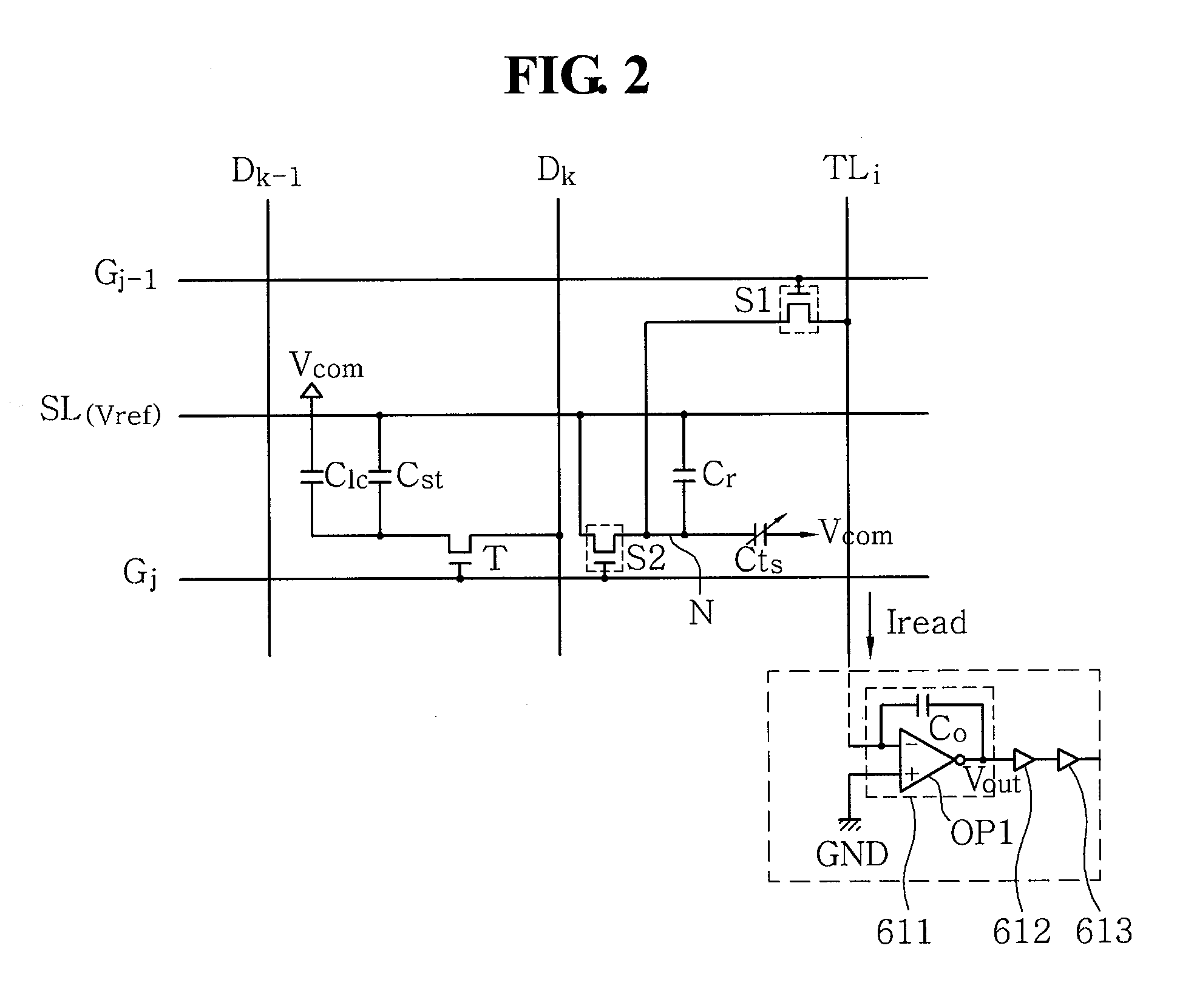
[0117]As shown in Table 1 and FIG. 9, when the cell gap in the TSP 100 is 0.6 cm, the output voltage Vout of the integration circuit 611 is 0.34V. However, when the cell gap in the TSP 100 is reduced as 0.1 μm by a user's touch action, the output voltage Vout of the integration circuit 611 is 1.53V.

[0118]In FIG. 9, Line X shows results based on the operation of the TSP 100 acc...

second embodiment

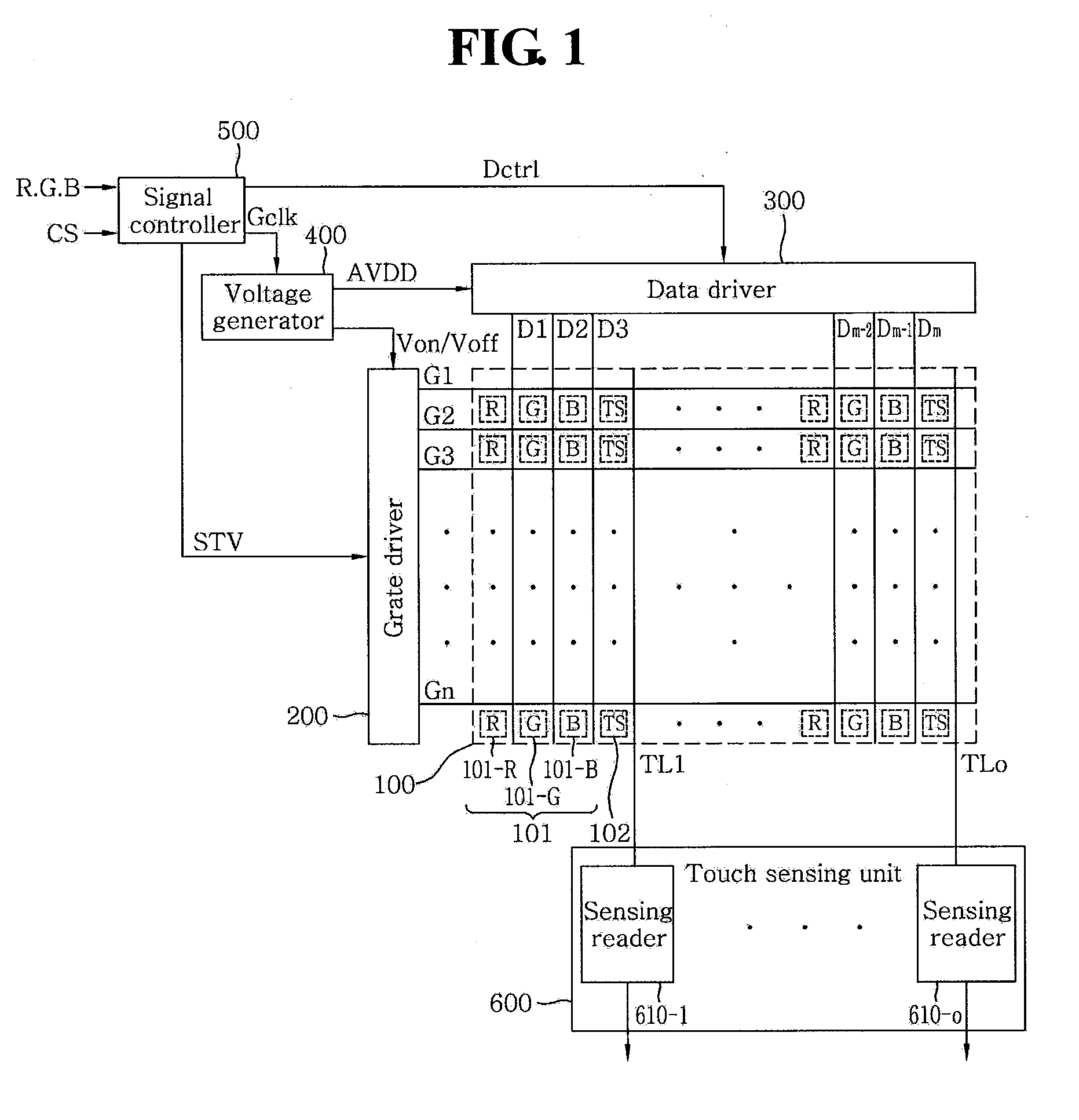
[0136]Referring to FIGS. 13 to 20, the touch screen apparatus further includes a gate clock generator 700, which receives a first vertical synchronization start signal STV and a driving clock signal CPV from the signal controller 500 and receives a gate turn-on voltage Von and a gate turn-off voltage Voff from the driving voltage generator 400 to provide a second vertical synchronization start signal STVP, a gate clock signal CKV, and an inverse gate clock signal CKVB to the gate driver 200. Here, the gate driver 200 includes a plurality of stages (not shown). The stages are connected to the gate lines G1 to Gn, respectively. The stages sequentially provide a gate turn-on signal SVg+ to some of the gate lines G1 to Gn according to the second vertical synchronization start signal STVP, the gate clock signal CKV, the inverse gate clock signal CKVB, and the signal of the previous stage. The stages provide a gate turn-off signal SVg− to the remaining gate lines G1 to Gn to which the ga...


PUM


Abstract

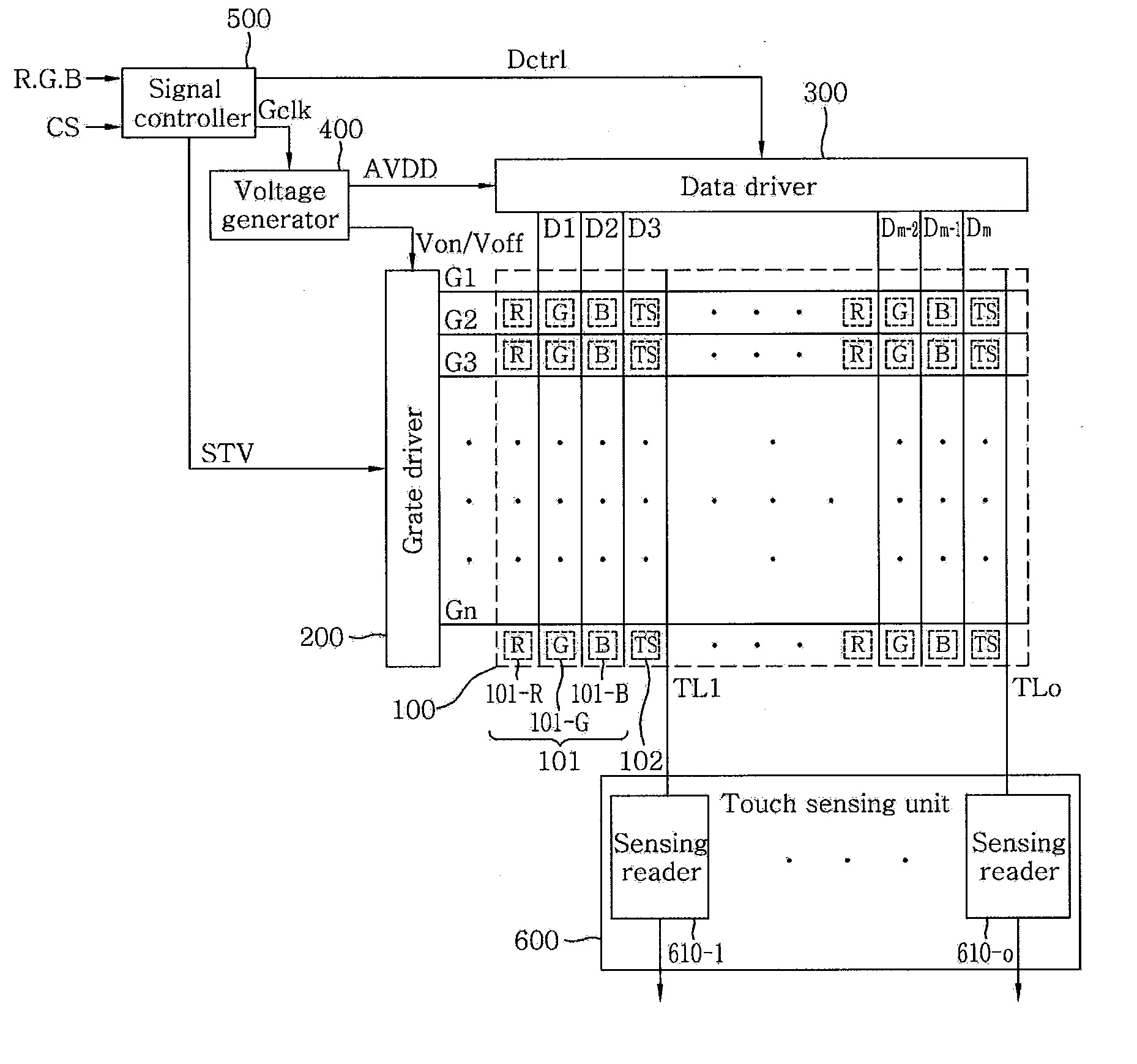
There is provided a touch screen apparatus capable of detecting the presence a touch action and a position in a touch region depending on a change in electrical energy of one node of a touch sensor. A touch screen apparatus according to the present invention includes a plurality of pixels for displaying images and a plurality of touch sensors. Each of the plurality of touch sensors includes a first node being provided an electrical energy; a sensor capacitor for changing the electric potential energy of the first node depending on presence a touch action; a first switch for providing a sensing signal to the touch line controlled by the electrical energy of the first node; and a second switch for providing the electrical energy to the first node.

Description

[0001]This application claims benefit of priority to Korean Patent application No. 10-2007-0120766, filed on Nov. 26, 2007 under 35 U.S.C. 119, the contents of which are herein incorporated by reference in their entirety.BACKGROUND OF THE INVENTION[0002]1. Field of the Invention[0003]The present invention relates to a touch screen apparatus, and more particularly, to a touch screen apparatus for detecting a touch position by sensing a change in capacitance caused by a user's input operation (touch).[0004]2. Description of the Related Art[0005]In general, a touch screen panel (TSP) is used as an input unit. A resistance-type touch screen apparatus is widely used as such touch screen panel. That is, resistance in the touched region is changed by the force applied when a user touches the touch screen panel. A touch position in the touch screen apparatus can be detected by sensing a resistance change.[0006]Such a resistance-type touch screen panel includes an upper substrate and a lower...

Claims


Application Information

Patent Timeline
IPC IPC(8): G06F3/045
CPCG06F3/044G06F3/0416G06F3/0446G06F3/0447G06F3/0412H03K17/962
Inventor TAKAHASHI, SEIKILEE, BYOUNG-JUNLEE, JUN-PYO
Owner SAMSUNG DISPLAY CO LTD
Learn More