Semiconductor laser apparatus and optical amplifier apparatus
a semiconductor laser and amplifier technology, applied in semiconductor lasers, instruments, optical elements, etc., can solve the problems of difficult to inject a current directly through the silicon waveguide into the compound semiconductor, difficult to apply the same to actual devices, and difficult to amplify light in the inside of silicon materials
- Summary
- Abstract
- Description
- Claims
- Application Information
AI Technical Summary
Benefits of technology
Problems solved by technology
Method used
Image

Examples
first embodiment
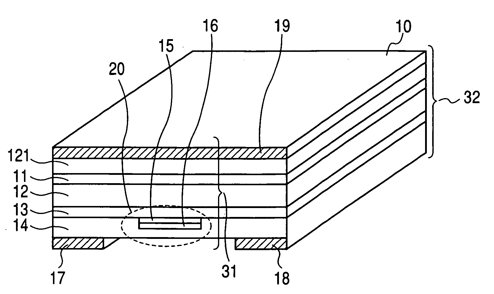
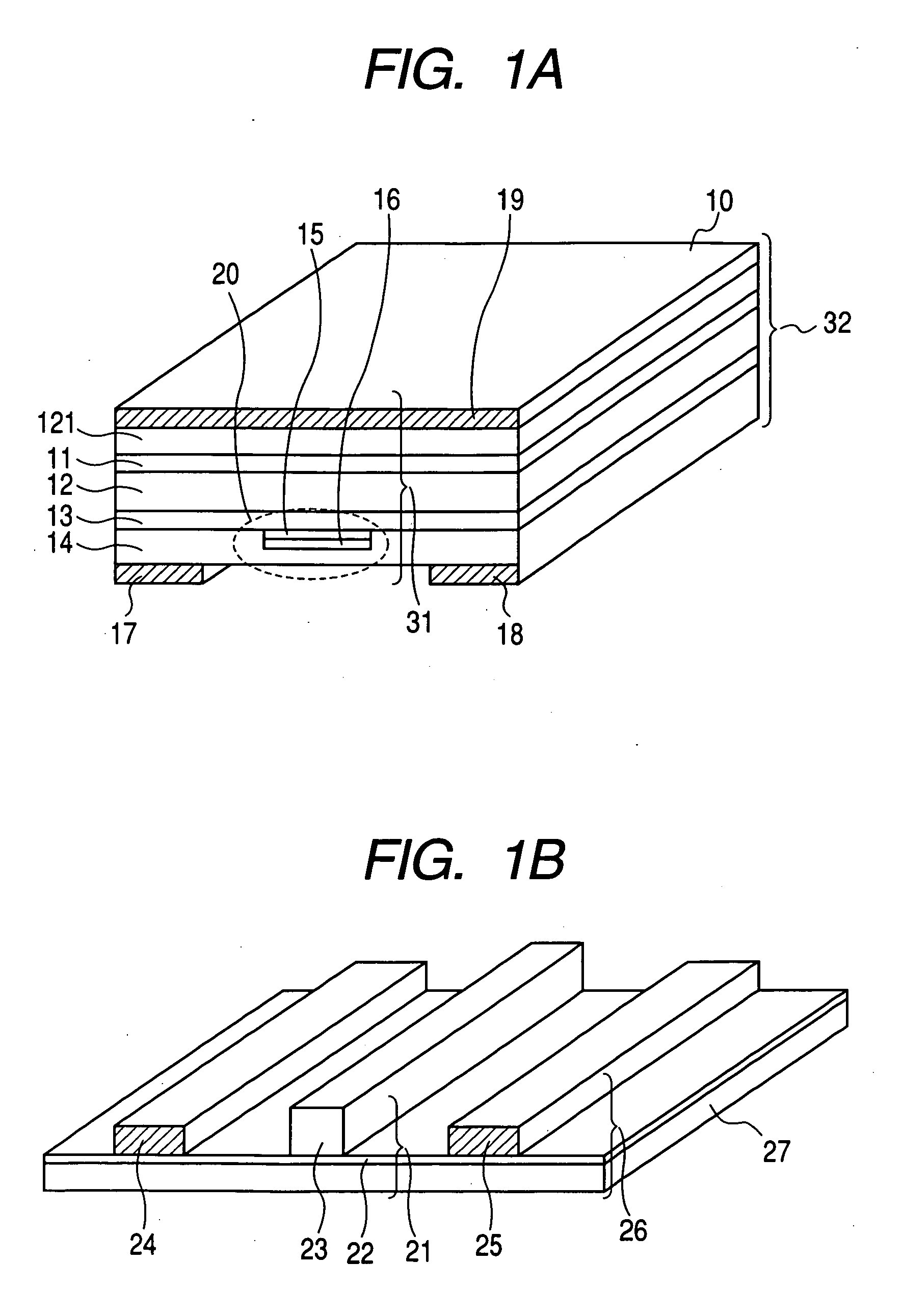
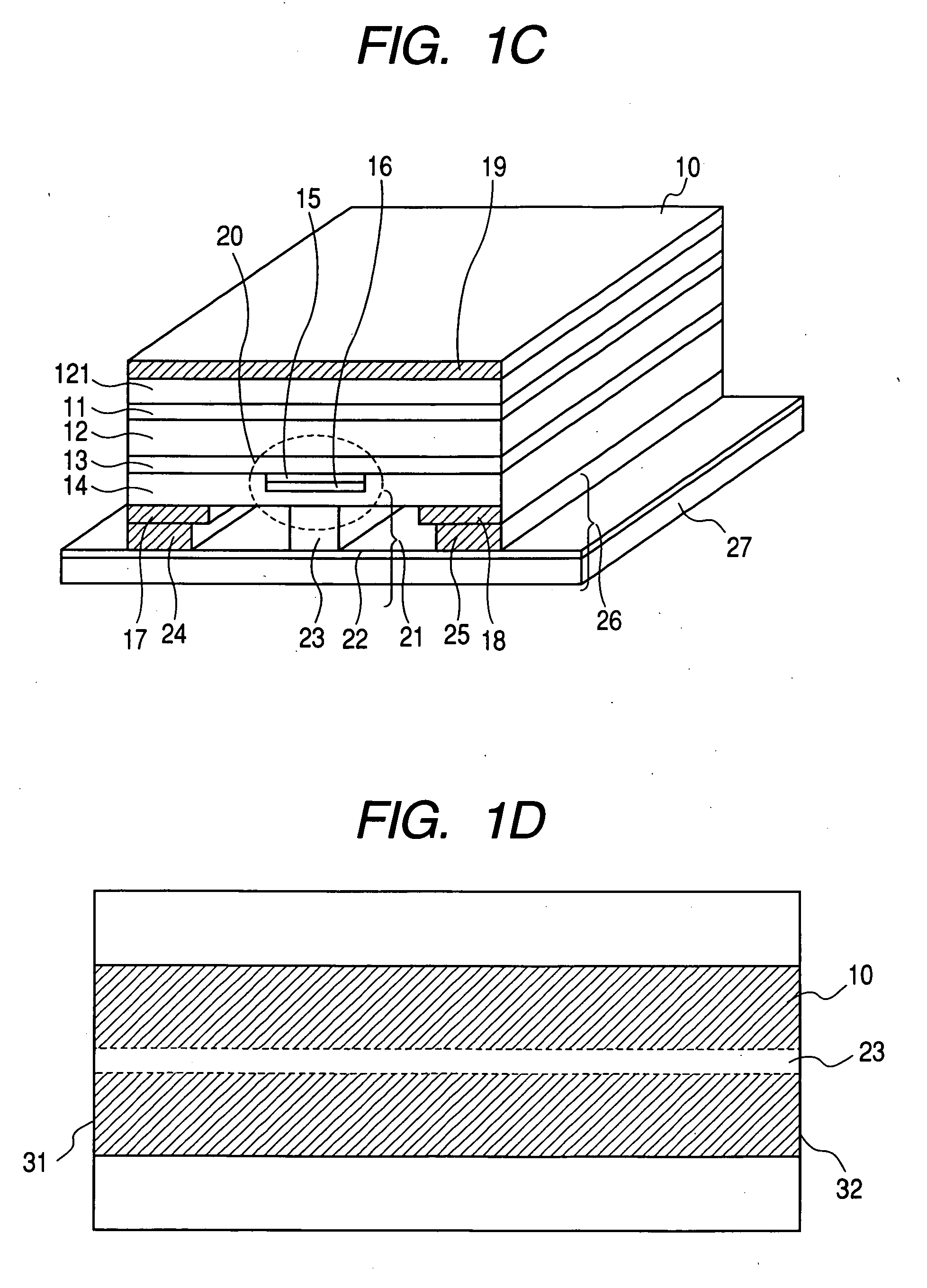
[0071]FIGS. 1A and 1B show a first embodiment of the invention. This embodiment is an example of forming a laser resonator between end faces 31 and 32 to attain laser oscillation. FIG. 1A is a perspective view of a compound semiconductor, FIG. 1B is a perspective view of an SOI (Silicon-On-Insulator) substrate, FIG. 1C is an entire perspective view, and FIG. 1D is an entire upper plan view. FIG. 7 is a view showing a current injection path in the entire upper plan view.
[0072]As shown in FIG. 1A, on a compound semiconductor substrate 121 using InP as a material, an n-type semiconductor layer 11 (for example, a first clad layer here and hereinafter), a semiconductor active layer 12, and a p-type semiconductor layer 13 (for example, a second clad layer here and hereinafter) are disposed. Further, a tunneling junction structure 20, a p-type semiconductor layer 15 doped at a concentration higher than that of the p-type semiconductor layer 13, an n-type semiconductor layer 16, and an n-ty...
second embodiment
[0083]FIG. 2 shows a second embodiment of the invention. This embodiment is an example of forming a laser resonator between end faces 61, 62 to attain laser oscillation. FIG. 2A is a perspective view of a compound semiconductor, FIG. 2B is a perspective view of an SOI (Silicon-On-Insulator) substrate, FIG. 2C is a perspective view for a compound semiconductor member and an SOI substrate in combination, for example, an entire semiconductor laser apparatus, and FIG. 2D is an entire upper plan view thereof. FIG. 8 is a view showing a current injection path in the entire perspective view.
[0084]As shown in FIG. 2A, the compound semiconductor has a semiconductor active layer 42 formed in a stripe shape to a portion on an insulative semiconductor layer 41 above a compound semiconductor substrate 40 made of InP, an insulative semiconductor layer 43 for confining a current to the active layer, an n-doped contact layer 44, and a p-type doped contact layer 45, in which an electrode 46 is dispo...
third embodiment
[0093]FIG. 3 shows a third embodiment of the invention. In this embodiment, a distributed feedback type laser is formed by additionally forming a diffraction grating to the compound semiconductor member described in the first embodiment.
[0094]As shown in FIG. 3A, in a compound semiconductor member 80 using InP as a material, a diffraction grating 71 was at first formed to a portion of the n-type semiconductor layer 11 on an active layer. Then, the compound semiconductor member 80 is completed by way of the steps identical with those in the first embodiment.
[0095]As shown in FIG. 3B, a silicon member 26 is completed by way of the steps identical with those in the first embodiment.
[0096]Then, as shown in FIG. 3C, a semiconductor laser apparatus is completed by the steps identical with those in the first embodiment.
[0097]In this embodiment, since the diffraction grating is present, the end face reflection mirror is not necessary. Accordingly, as shown in FIG. 3D, it can be also constit...
PUM
 Abstract
Description
Claims
Application Information
 - R&D
- Intellectual Property
- Life Sciences
- Materials
- Tech Scout
- Unparalleled Data Quality
- Higher Quality Content
- 60% Fewer Hallucinations
Browse by: Latest US Patents, China's latest patents, Technical Efficacy Thesaurus, Application Domain, Technology Topic, Popular Technical Reports.
© 2025 PatSnap. All rights reserved.Legal|Privacy policy|Modern Slavery Act Transparency Statement|Sitemap|About US| Contact US: help@patsnap.com