Memory and manufacturing method thereof
a manufacturing method and memory technology, applied in the direction of semiconductor devices, electrical devices, transistors, etc., can solve problems affecting the correctness of overall data reading, and achieve the effect of increasing the electron storage space and increasing the concentration of electron storag
- Summary
- Abstract
- Description
- Claims
- Application Information
AI Technical Summary
Benefits of technology
Problems solved by technology
Method used
Image
Examples
first embodiment
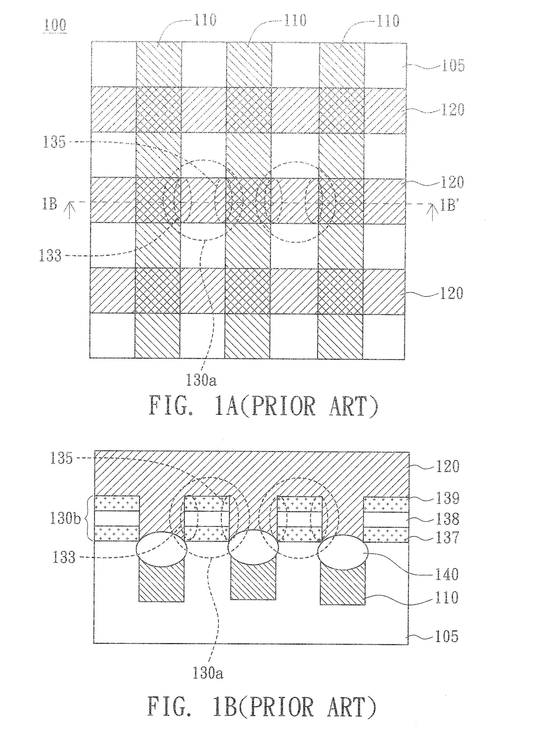
[0020]Referring to FIGS. 2A˜2B. FIG. 2A is a partial top view of a memory according to a first embodiment of the invention. FIG. 2B is a cross-sectional view of the memory along the cross-sectional line 2B˜2B′ of FIG. 2A. In FIGS. 2A˜2B, the memory 200 includes a substrate 210, a number of bit lines 220, a number of word lines 230, a number of oxide-nitride-oxide (ONO) structures 240, a number of isolation layers 250, a number of memory cells 215 (enclosed in larger dotted circles in FIG. 2A and FIG. 2B), a number of first bit storage nodes 217a, and a number of second bit storage nodes 217b. The bit lines 220 are disposed in parallel, formed in the substrate 210, and positioned near the surface of the substrate 210. The word lines 230 are disposed in parallel and formed on the substrate 210. Furthermore, the word lines 230 are crossed with but not perpendicular to the bit lines 220. That is, an acute angle θ is contained between the word lines 230 and the bit lines 220. In the pres...
second embodiment
[0029]Referring to FIGS. 4A˜4B. FIG. 4A is partial top view of a memory according to a second embodiment of the invention. FIG. 4B is a cross-sectional view of the memory along the cross-sectional line 4B˜4B′ of FIG. 4A. In FIGS. 4A˜4B, the memory 300 includes a substrate 310, a number of bit lines 320, a number of word lines 330, a oxide-nitride-oxide (ONO) layer 340, a number of memory cells 315 (enclosed in larger dotted circles in FIG. 4A and FIG. 4B), a number of first bit storage nodes 317a, and a number of second bit storage nodes 317b. The bit lines 320 are disposed in parallel formed in the substrate 310, and positioned near the surface of the substrate 310. The word lines 330 are disposed in parallel and formed on the substrate 310. Furthermore, the word lines 330 are crossed with but not perpendicular to the bit lines 320. That is, an acute angle α is contained between the word lines 330 and the bit lines 320. In the present embodiment of the invention, the acute angle α ...
PUM
 Abstract
Description
Claims
Application Information
 - R&D
- Intellectual Property
- Life Sciences
- Materials
- Tech Scout
- Unparalleled Data Quality
- Higher Quality Content
- 60% Fewer Hallucinations
Browse by: Latest US Patents, China's latest patents, Technical Efficacy Thesaurus, Application Domain, Technology Topic, Popular Technical Reports.
© 2025 PatSnap. All rights reserved.Legal|Privacy policy|Modern Slavery Act Transparency Statement|Sitemap|About US| Contact US: help@patsnap.com


