Clock signal control method in the common clock and integrated circuit device
a clock signal and integrated circuit technology, applied in the direction of generating/distributing signals, pulse automatic control, instruments, etc., can solve the problems of clock signal loss, clock signal loss, clock signal cannot be controlled, clock signal itself falls to a self-oscillation frequency, etc., to facilitate circuit design using an integrated circuit devi
- Summary
- Abstract
- Description
- Claims
- Application Information
AI Technical Summary
Benefits of technology
Problems solved by technology
Method used
Image

Examples
first embodiment
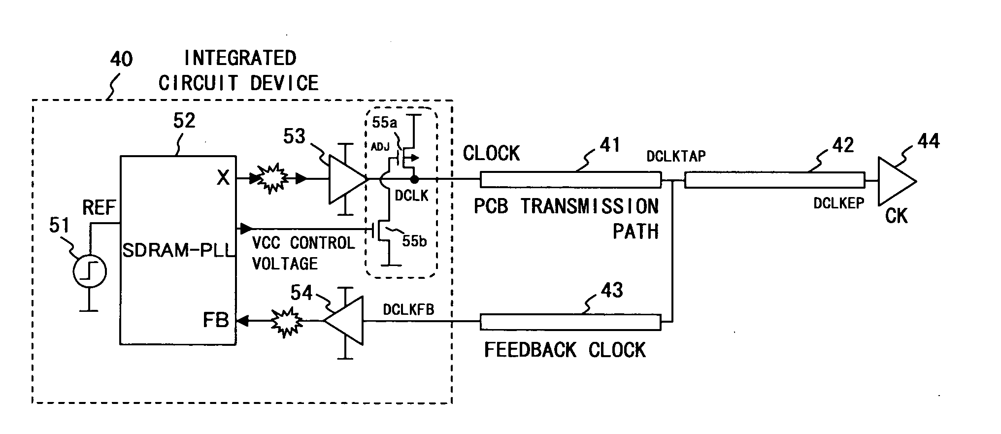
[0052]FIG. 4 is a diagram explaining the configuration of the integrated circuit device of the first embodiment. In FIG. 4, 40 represents an integrated circuit device (hereinafter referred to as “chip”) loaded on a printed circuit board (PCB), 41-43 are transmission paths of a clock signal formed on the PCB, and 44 is a receiver circuit in a circuit to which a clock signal is input (the device serves as a load).
[0053]The chip (integrated circuit device) 40 is loaded with an I / F supporting the common clock system and has a configuration comprising an oscillator 51 for generating a reference clock signal REF serving as a reference, an SDARM-PLL 52 loaded with a PLL circuit (PLL macro), a driver circuit 53 for amplifying and outputting the clock signal output from an X-terminal of the SDRAM-PLL 52, a receiver circuit for inputting and shaping the clock signal from the PCB, and a shift circuit 55 provided at the output side of the driver circuit 53.
[0054]The shift circuit 55 is a circui...
second embodiment
[0076]In the first embodiment, VCO control voltage is used for driving the shift circuit 55. However, if wiring for outputting the VCO control voltage, which is crucial to the PLL macro, is installed, it is probable that undesirable situations such as noise being mixed in the VCO control voltage and an influence on the time constant of LPF 1113 that determines the characteristics that follow may arise. Hence, the second embodiment employs a lock signal instead of the VCO control voltage.
[0077]In the second embodiment, components that are the same as or essentially similar to those in the first embodiment are assigned the same reference numerals. Therefore, the explanation is provided with the focus on the parts that are different from the first embodiment. This also applies to the other embodiments explained later.
[0078]FIG. 8 is a diagram explaining the configuration of the integrated circuit device according to the second embodiment. The second embodiment comprises a shift circuit...
third embodiment
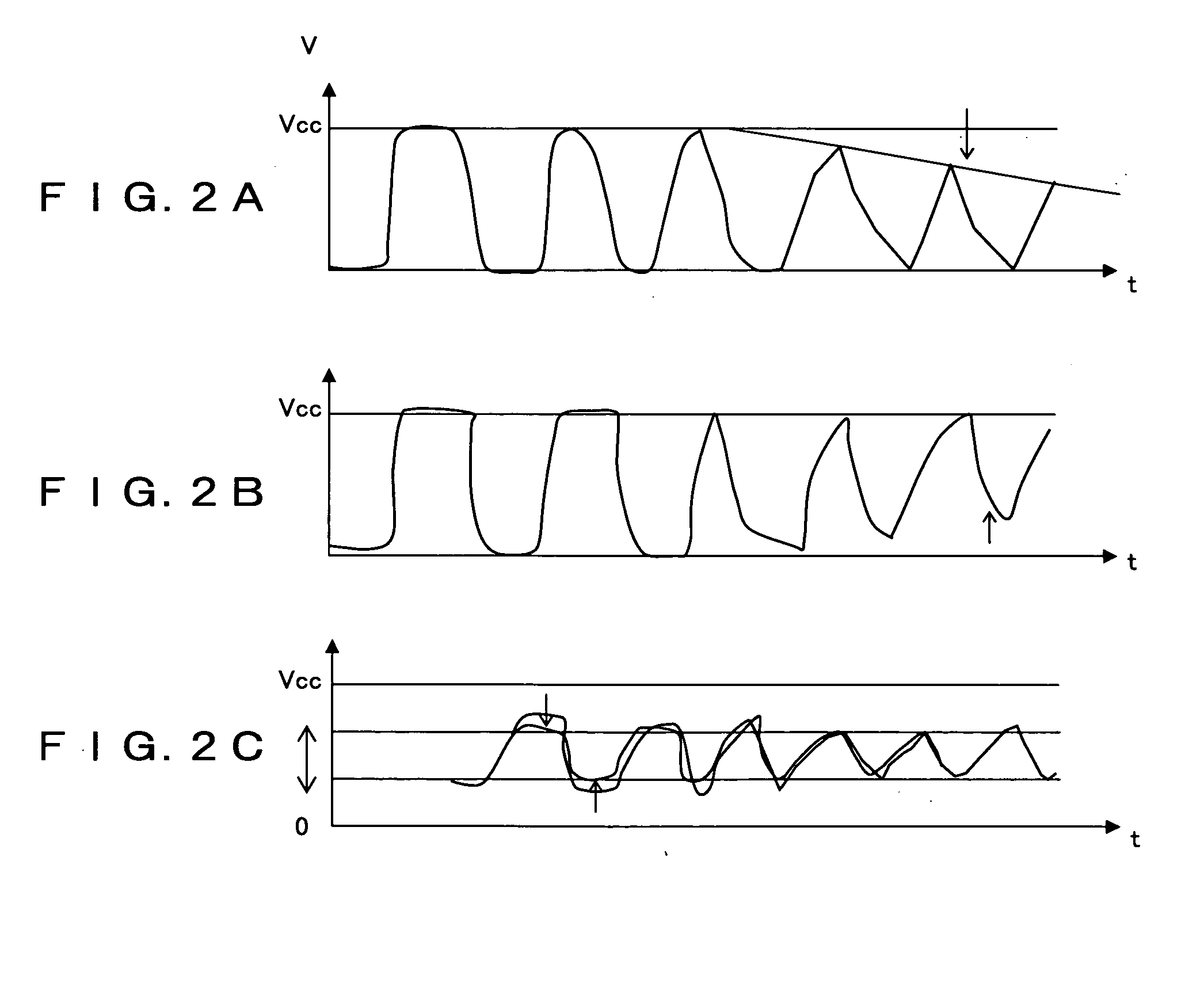
[0084]When the external I / O voltage becomes low—that is, when the amplitude of the clock signal DCLK is reduced—it is fundamentally difficult to shape the waveform of the clock signal DCLK that is propagated in the transmission path even though the driving capacity of the driver circuit 53 is improved. In many cases, the shape of the waveform is roughly determined by the branch shape of the PCB transmission path and the number of loads, and waveform shaping via adjustments other than increasing the external I / O voltage is difficult.
[0085]By shifting the voltage level using the shift circuit 55 or 80, it is possible to shape the waveform of the clock signal DCLK. However, as explained above, since the waveform of the clock signal DCLK is roughly determined by the branch shape of the PCB transmission path and the number of loads, the amount of shift to the shape of the waveform varies depending on the PCB where the chip 40 is loaded. The third embodiment enables fine adjustment of the...
PUM
 Abstract
Description
Claims
Application Information
 - R&D
- Intellectual Property
- Life Sciences
- Materials
- Tech Scout
- Unparalleled Data Quality
- Higher Quality Content
- 60% Fewer Hallucinations
Browse by: Latest US Patents, China's latest patents, Technical Efficacy Thesaurus, Application Domain, Technology Topic, Popular Technical Reports.
© 2025 PatSnap. All rights reserved.Legal|Privacy policy|Modern Slavery Act Transparency Statement|Sitemap|About US| Contact US: help@patsnap.com