Electronic device having black layers
a technology of electronic devices and layers, applied in semiconductor devices, instruments, optics, etc., can solve the problems of increasing the thickness of the module, increasing the cost, and affecting the use of the display
- Summary
- Abstract
- Description
- Claims
- Application Information
AI Technical Summary
Benefits of technology
Problems solved by technology
Method used
Image
Examples
Embodiment Construction
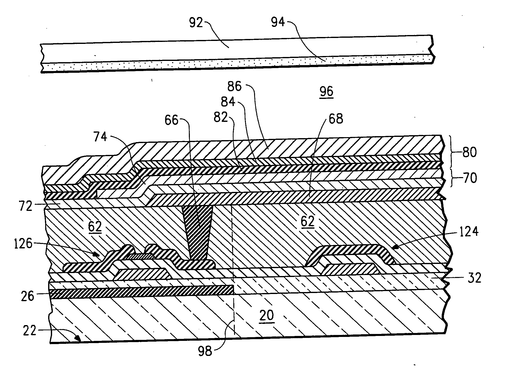
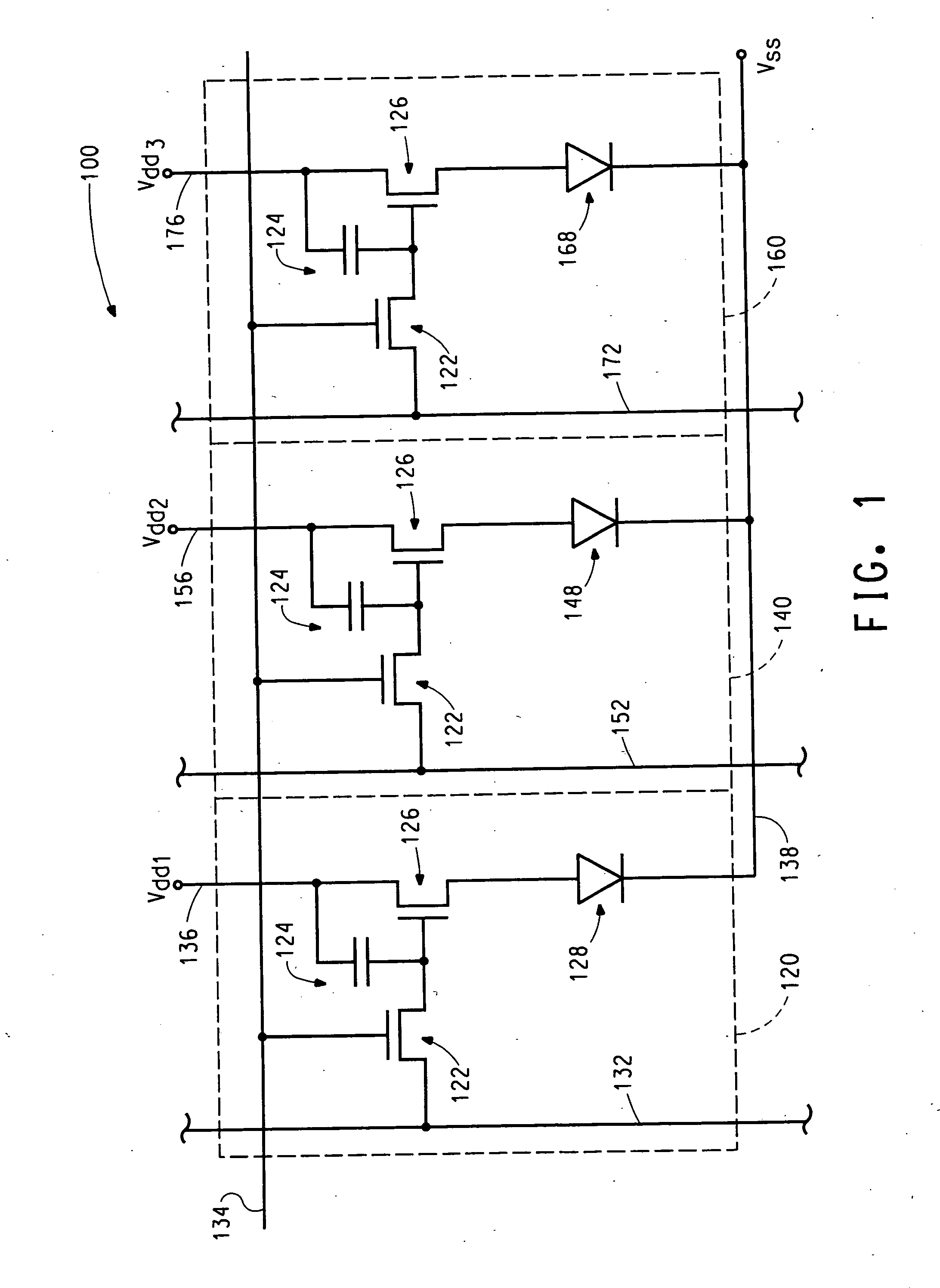
[0022] In a first aspect, an electronic device can include a control circuit of a pixel, a first black layer including an opening, and a second black layer. The control circuit can lie at an elevation between the first black layer and the second black layer.
[0023] In one embodiment of the first aspect, the pixel can include a first electrode. The first electrode can include a portion of the second black layer, and the first electrode can be electrically coupled to the control circuit. In a particular embodiment, the pixel can further include a second electrode that is electrically connected to the control circuit. In another embodiment, the electronic device can further include a substrate including a user surface that lies closer to the first black layer as compared to the second black layer.
[0024] In still another embodiment of the first aspect, the opening within the first black layer can correspond to a user radiation path of the pixel, wherein at least a portion of the contro...
PUM
 Abstract
Description
Claims
Application Information
 - R&D
- Intellectual Property
- Life Sciences
- Materials
- Tech Scout
- Unparalleled Data Quality
- Higher Quality Content
- 60% Fewer Hallucinations
Browse by: Latest US Patents, China's latest patents, Technical Efficacy Thesaurus, Application Domain, Technology Topic, Popular Technical Reports.
© 2025 PatSnap. All rights reserved.Legal|Privacy policy|Modern Slavery Act Transparency Statement|Sitemap|About US| Contact US: help@patsnap.com


