Display apparatus
a technology of display apparatus and display screen, which is applied in the field of display screen, can solve the problems of reducing the light emission efficiency of the organic electroluminescent device itself, reducing the light extraction intensity of the subpixel of emitted blue and green lights, etc., and achieves the effects of reducing the intensity of the light, reducing the light emission efficiency, and maximizing the optical design
- Summary
- Abstract
- Description
- Claims
- Application Information
AI Technical Summary
Benefits of technology
Problems solved by technology
Method used
Image
Examples
first embodiment
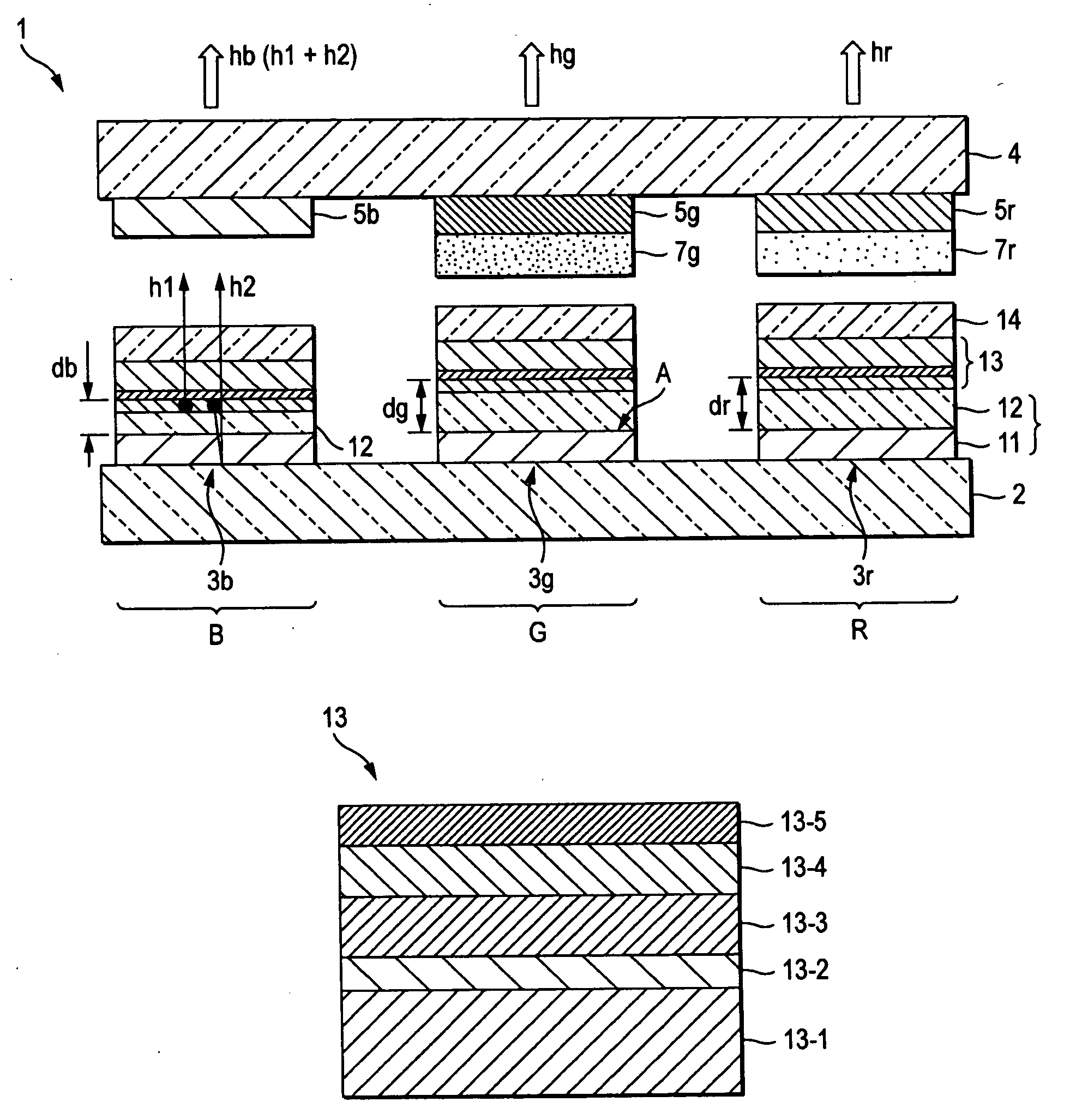
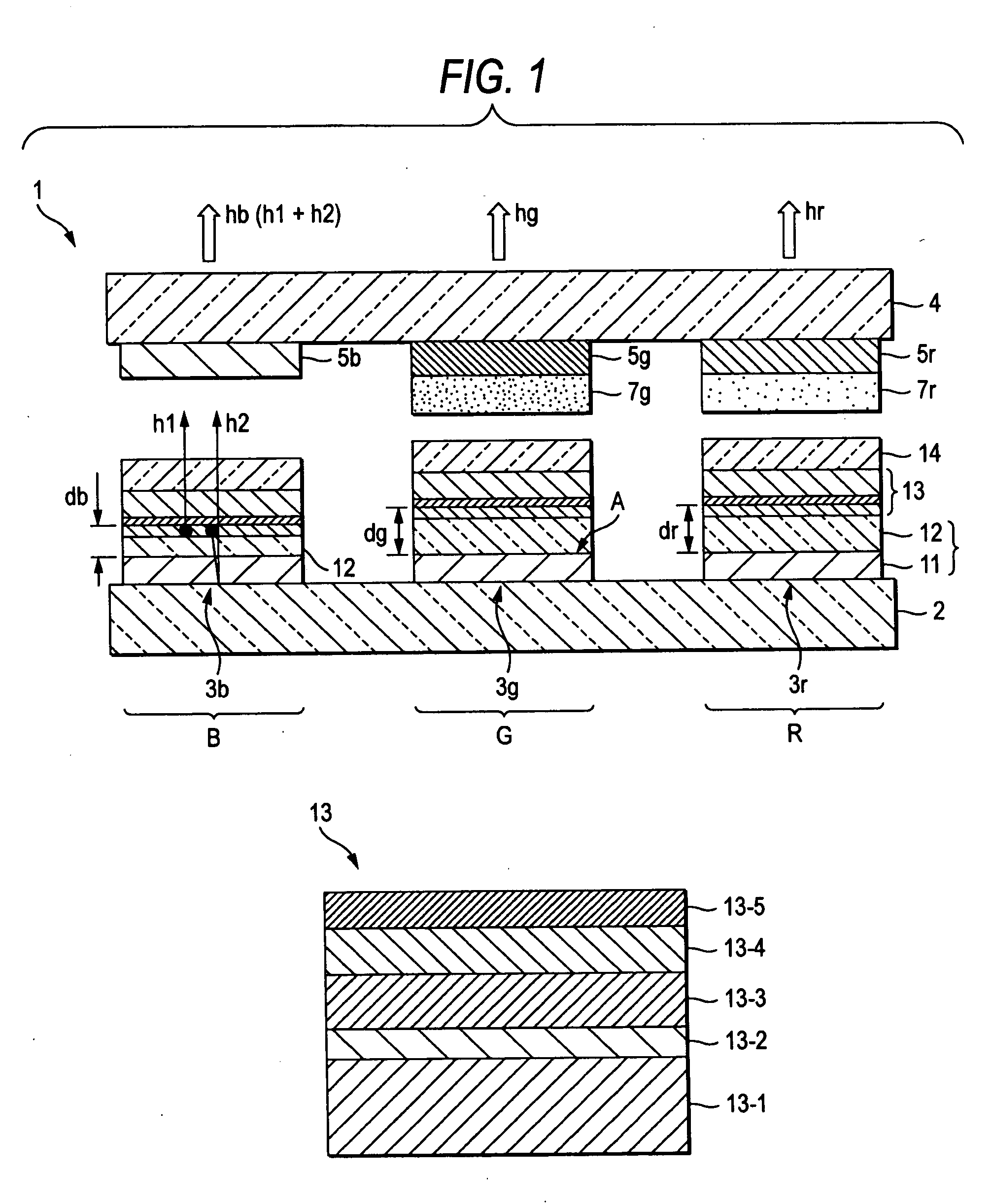
[0026]FIG. 1 is a diagram showing the cross sectional configuration of a display apparatus of a first embodiment. A display apparatus 1 of FIG. 1 includes a plurality of light-emitting devices 3b, 3g, and 3r disposed on a substrate 2. Above these light-emitting devices 3b, 3g, and 3r, a sealing substrate 4 is so disposed as to oppose to the substrate 2. The sealing substrate 4 is provided with, on the surface facing the light-emitting devices 3b, 3g, and 3r, color filter layers 5b, 5g, and 5r corresponding to the light-emitting devices 3b, 3g, and 3r, respectively. A part of the color filters, i.e., the color filters 5g and 5r in this example, is provided with color conversion layers 7g and 7r corresponding to the light-emitting devices 3g and 3r, respectively. Between the substrate 2 and the sealing substrate 4, a resin (not shown) is filled so that the resulting display apparatus 1 is structured completely solid with the components sealed together, i.e., the light-emitting element...
second embodiment
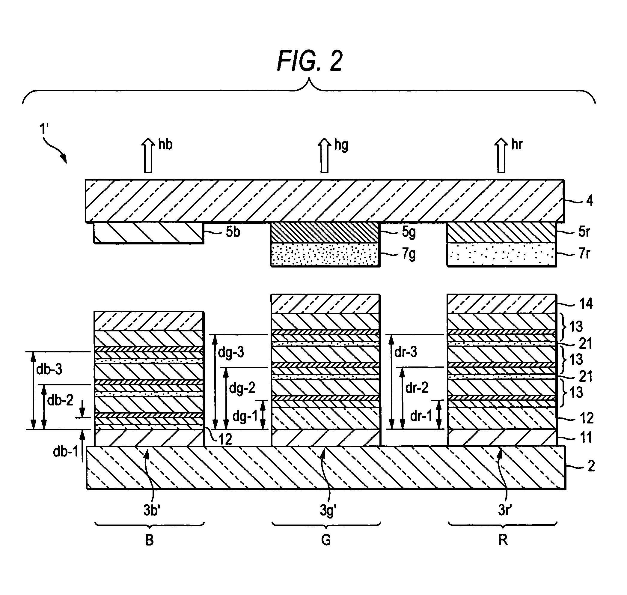
[0053]FIG. 2 is a cross sectional diagram showing the configuration of a display apparatus of a second embodiment. A display apparatus 1′ of FIG. 2 is different from the display apparatus 1 described by referring to FIG. 1 in the first embodiment in the respect that a plurality of functional layers 13 are accumulated via intermediate electrode layers 21 between the reflective electrode layer 11 and the light transmissive electrode layer 14, and the remaining configuration is similar to each other. The drawing shows an accumulation of the three functional layers 13. This is not the only possibility, and two or more functional layers 13 are good enough, or four or more layers will also do.
[0054] The functional layers 13 and the intermediate layers 21 are each provided as a common layer for the subpixels B, G, R, and may be solidly formed on the substrate 2. For convenient reference, the drawing shows the state that the functional layers 13 and the intermediate electrode layers 21 are...
example 1
[0067] In the below, an example 1 and comparison examples 1 and 2 of the invention are described.
PUM
 Abstract
Description
Claims
Application Information
 - R&D
- Intellectual Property
- Life Sciences
- Materials
- Tech Scout
- Unparalleled Data Quality
- Higher Quality Content
- 60% Fewer Hallucinations
Browse by: Latest US Patents, China's latest patents, Technical Efficacy Thesaurus, Application Domain, Technology Topic, Popular Technical Reports.
© 2025 PatSnap. All rights reserved.Legal|Privacy policy|Modern Slavery Act Transparency Statement|Sitemap|About US| Contact US: help@patsnap.com


