Voltage level translator
- Summary
- Abstract
- Description
- Claims
- Application Information
AI Technical Summary
Benefits of technology
Problems solved by technology
Method used
Image
Examples
Example
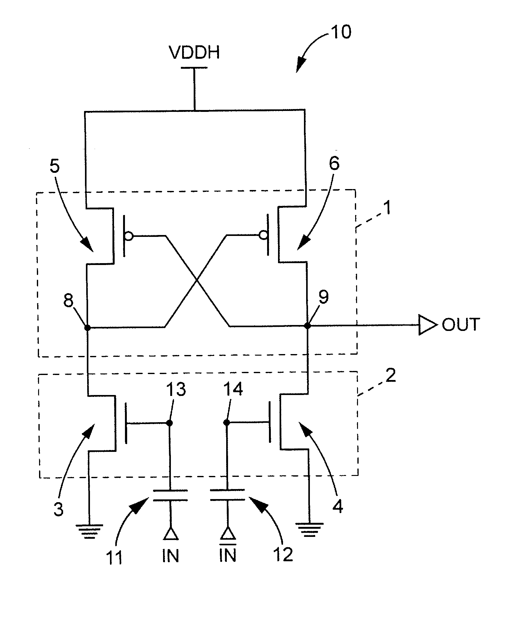
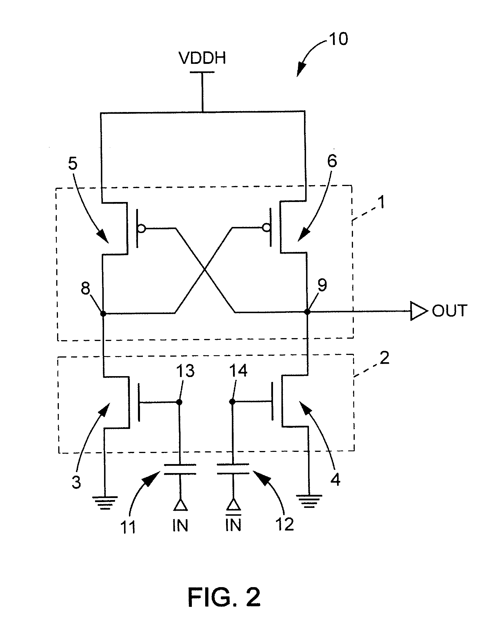
[0080] In the second embodiment, the first and second boosting means respectively comprise first and second capacitor arranged transistors 11′, 12′.
[0081] The n-channel transistors 3, 4 are respectively connected at their drain terminals to two p-channel transistors 5, 6 via connection nodes 8, 9.
[0082] Furthermore, a first p-channel transistor 6 connected to the first n-channel transistor 4 via a first connection node 9 is driven by the voltage of a second connection node 8. A second p-channel transistor 5 connected to the second n-channel transistor 3 via the second connection node 8 is driven by the voltage of the first connection node 9.
[0083] A digital output signal OUT is read at the first connection node 9.
[0084] If, as shown in FIG. 4, the digital input signal IN rises up to a low voltage level VDDL at a first time t1, the voltage V13 of the second control node 13 is boosted beyond the low voltage level VDDL, thus allowing to improve the operating of the second n-channel...
PUM
 Abstract
Description
Claims
Application Information
 - R&D Engineer
- R&D Manager
- IP Professional
- Industry Leading Data Capabilities
- Powerful AI technology
- Patent DNA Extraction
Browse by: Latest US Patents, China's latest patents, Technical Efficacy Thesaurus, Application Domain, Technology Topic, Popular Technical Reports.
© 2024 PatSnap. All rights reserved.Legal|Privacy policy|Modern Slavery Act Transparency Statement|Sitemap|About US| Contact US: help@patsnap.com


