Optical modulator and a method for adapting an optical modulator

a technology of optical modulator and optical modulator, applied in the field of optical modulator, can solve the problems of low characteristic impedance of electrical transmission line, affecting the performance of optical modulator, so as to avoid the high impedance level of passive waveguide

Active Publication Date: 2007-01-11
II VI DELAWARE INC
View PDF5 Cites 19 Cited by
  • Summary
  • Abstract
  • Description
  • Claims
  • Application Information

AI Technical Summary

Benefits of technology

[0034] An advantage with the present invention is the problem with high impedance level in the passive waveguide is avoided.
[0035] An advantage with a first embodiment of the present invention is that the parasitic inductance found in the prior art is avoided.
[0036] An advantage with a second embodiment of the present invention is that the active segments make an inductive contribution to the passive transmission line.

Problems solved by technology

A disadvantage with this construction is that the characteristic impedance of the electrical transmission line is relatively low, usually around 25Ω.
Another disadvantage with this construction is that the electrical and optical wave may propagate with different velocities.
This effect will degrade the performance of the modulator.
This is particularly a problem for an EAM due to a typically high Cm.
2) The implementation of the passive transmission line as a co-planar line is sometimes disadvantageous.
Consequently, this implementation does not benefit from any inductive contribution from the active modulator segments.
This high impedance level is however not practical.
Betts approach improves the first disadvantage with the Walker design, as previously mentioned, and will also improve the second disadvantage by generalizing the implementation of the passive electrode to include other types of transmission lines besides the co-planar implementation suggested by Walker.
The third and fourth disadvantages with the Walker design are not improved by Betts.

Method used


Image

  • Optical modulator and a method for adapting an optical modulator
  • Optical modulator and a method for adapting an optical modulator
  • Optical modulator and a method for adapting an optical modulator

Examples


example 3

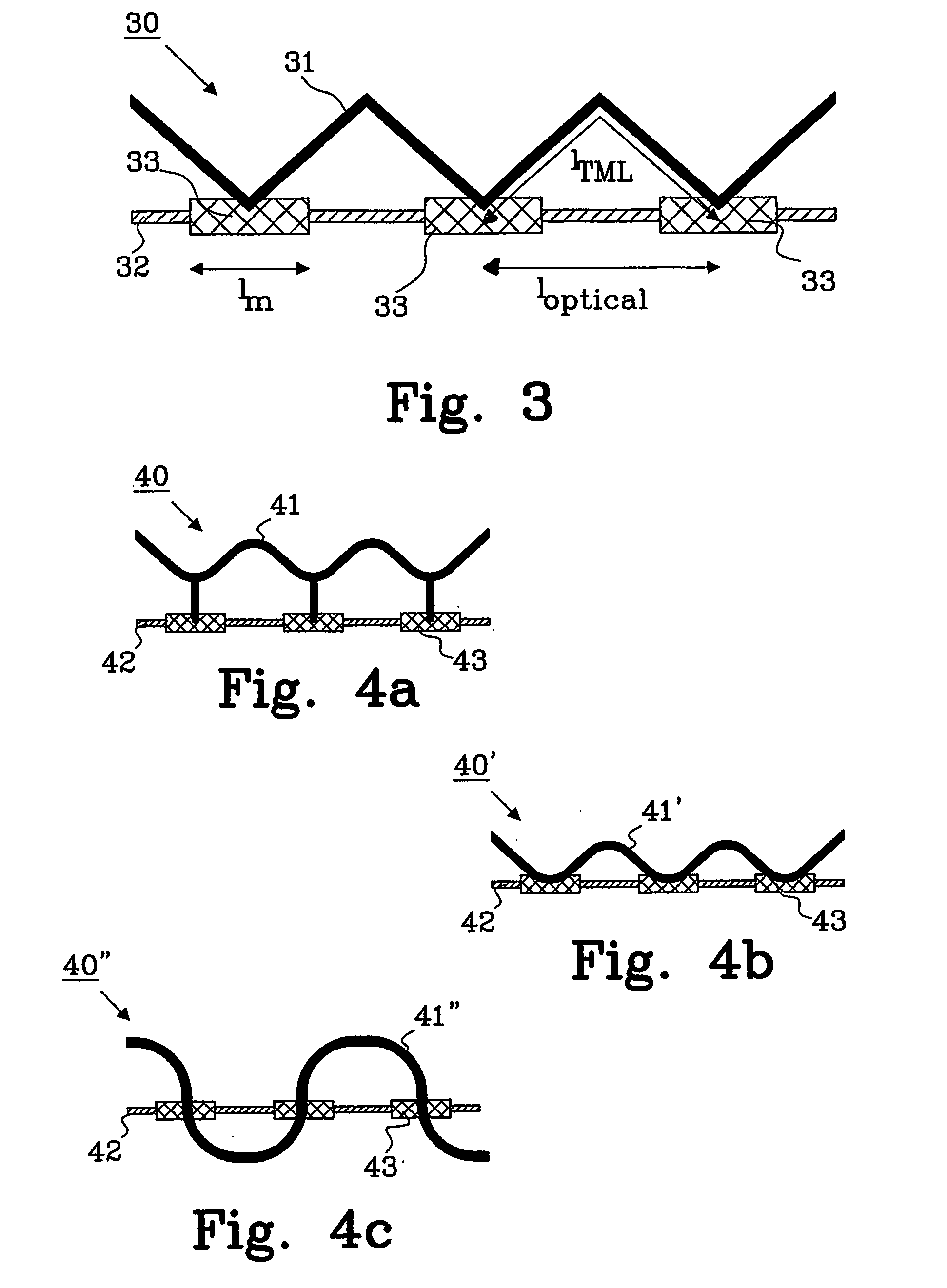
[0060] A TML implementation, corresponding to the present invention, as a microstrip on BCB with a maximum Zp of 75Ω, using a capacitively loaded line and having εr=2.7, εeff≈2.

[0061] With ZB=50Ω, then lTML / loptical=1.6 and Cm*lm / ls=130 pF / m.

[0062] A typical Cm for an electroabsorption modulator (EAM) is at least 700 pF / m, hence, lm / ls<0.185.

[0063] The design can be further improved by reducing the feed-lines (see Walker's design) or the conductive legs (see Betts' design) to a minimum. Ideally the modulator should be an integrated part of the passive waveguide, i.e. cascaded structure as illustrated in FIGS. 7a and 7b. This results in: (Cm-Cp)⁢lmls=n02-(np⁢lTMLloptical)2c0⁢ZB⁢n0=Ceff(11)

[0064] There are two reasons for this:

[0065] 1) The duty-cycle is improved by a ratio of ratio≈CmCm-Cp(12)

or typically 10% for an EAM implementation, where Cm≈700 pF / m, Cp≈70 pF / m.

[0066] 2) To avoid the implementation with conductive legs, which will avoid the parasitic inductance Ls as prev...


PUM

PropertyMeasurementUnit
impedanceaaaaaaaaaa
impedanceaaaaaaaaaa
heightaaaaaaaaaa

Abstract

The present invention relates to an optical modulator, divided into at least two active segments separated by at least one passive segment. The modulator comprises: an optical waveguide with an optical group index no having an optical signal propagating at an optical velocity vo, and a microwave transmission line with an electrical propagation index np, having an electrical signal propagating at an electrical velocity Ve. The electrical propagation index np of the unloaded microwave transmission line is lower than the optical group index no of the optical waveguide. The loading and length of the microwave transmission line are adjusted for a specific Bloch impedance and electrical velocity ve. The invention also relates to a method for adapting the impedance of an optical modulator.

Description

TECHNICAL FIELD [0001] The present invention relates to an optical modulator, more specifically a travelling wave optical modulator, as defined in the preamble of claim 1. The invention also relates to a method for adapting the impedance in an optical modulator as defined in the preamble of claim 6. BACKGROUND TO THE INVENTION [0002] There are generally two types of light intensity optical modulators, electro-optic (EO) and electroabsorption modulators (EAM). The EO modulator is based on interferometry where the refractive index is controlled by applying an external field, usually implemented in form of a Mach-Zender Interferometer (MZI), disclosed in a textbook by Koichi Waikita with the title “Semiconductor optical modulators” published by Kluwer Academic Publisher in USA, 1998 which is hereby incorporated as a reference in its entirety. Electroabsorption modulators are usually based on band to band absorption controlled by an external field through the Frans-Keldych or quantum co...

Claims


Application Information

Patent Timeline
Patent Type & Authority Applications(United States)
IPC IPC(8): G02F1/035G02F1/015
CPCG02F1/035G02F2201/16G02F2001/0157G02F1/0157
Inventor ERIKSSON, URBANLEWEN, ROBERT
Owner II VI DELAWARE INC
Why Eureka
Try Eureka