Method and system for compensation of non-uniformities in light emitting device displays

a technology of light emitting devices and non-uniformities, applied in the field of display technologies, can solve problems such as errors on visible light, different pixels may have different amounts of degradation, and non-uniformities in the illumination of a display

Active Publication Date: 2006-12-07
IGNIS INNOVATION
View PDF4 Cites 228 Cited by
  • Summary
  • Abstract
  • Description
  • Claims
  • Application Information

AI Technical Summary

Benefits of technology

[0012] It is an object of the invention to provide a method and system that obviates or mitigates at least one of the disadvantages of existing systems.

Problems solved by technology

Luminance non-uniformities in a display may also arise from natural differences in chemistry and performance from the OLED materials themselves.
However, there are several degradation factors which may cause errors on the visible light 36.
Depending on the usage of the display, different pixels may have different amounts of degradation.
Therefore, there will be an ever-increasing error between the required brightness of some pixels as specified by the luminance data in the video source 12, and the actual brightness of the pixels.
The result is that the desired image will not show properly on the display.
Not considering the inevitable issues of yield when integrating a light detector into each pixel, it is desirable to have a light detector which does not degrade itself, however such light detectors are costly to implement, and not compatible with currently installed TFT-LCD fabrication infrastructure.

Method used


Image

  • Method and system for compensation of non-uniformities in light emitting device displays
  • Method and system for compensation of non-uniformities in light emitting device displays
  • Method and system for compensation of non-uniformities in light emitting device displays

Examples


Embodiment Construction

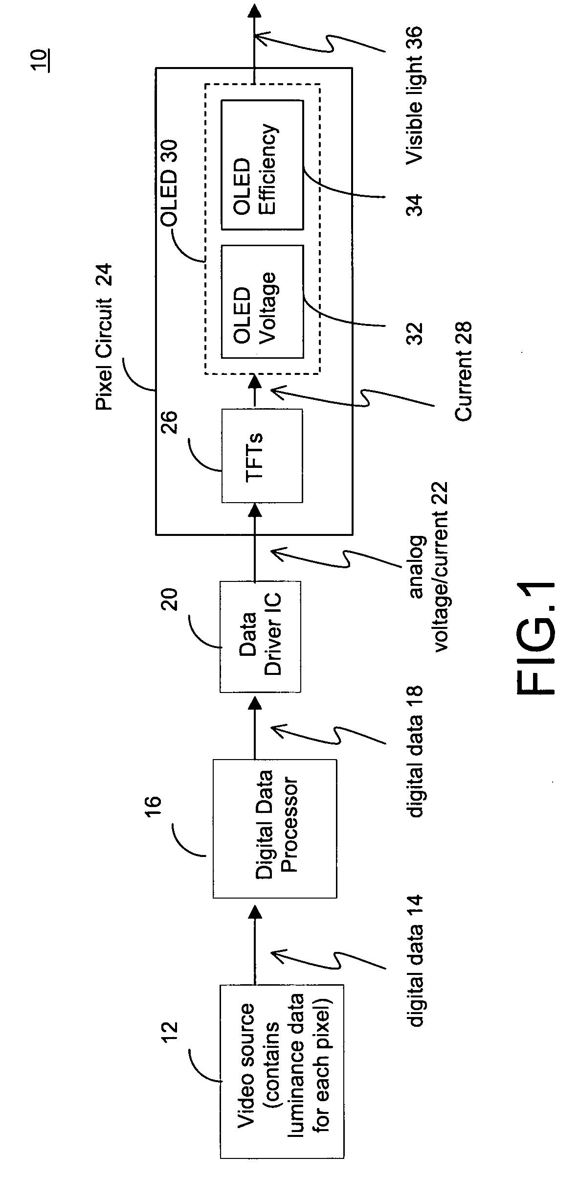
[0029] Embodiments of the present invention are described using an AMOLED display which includes a pixel circuit having TFTs and an OLED. However, the transistors in the pixel circuit may be fabricated using amorphous silicon, nano / micro crystalline silicon, poly silicon, organic semiconductors technologies (e.g. organic TFT), NMOS technology, CMOS technology (e.g. MOSFET), or combinations thereof. The transistors may be a p-type transistor or n-type transistor. The pixel circuit may include a light emitting device other than OLED. In the description below, “pixel” and “pixel circuit” may be used interchangeably.

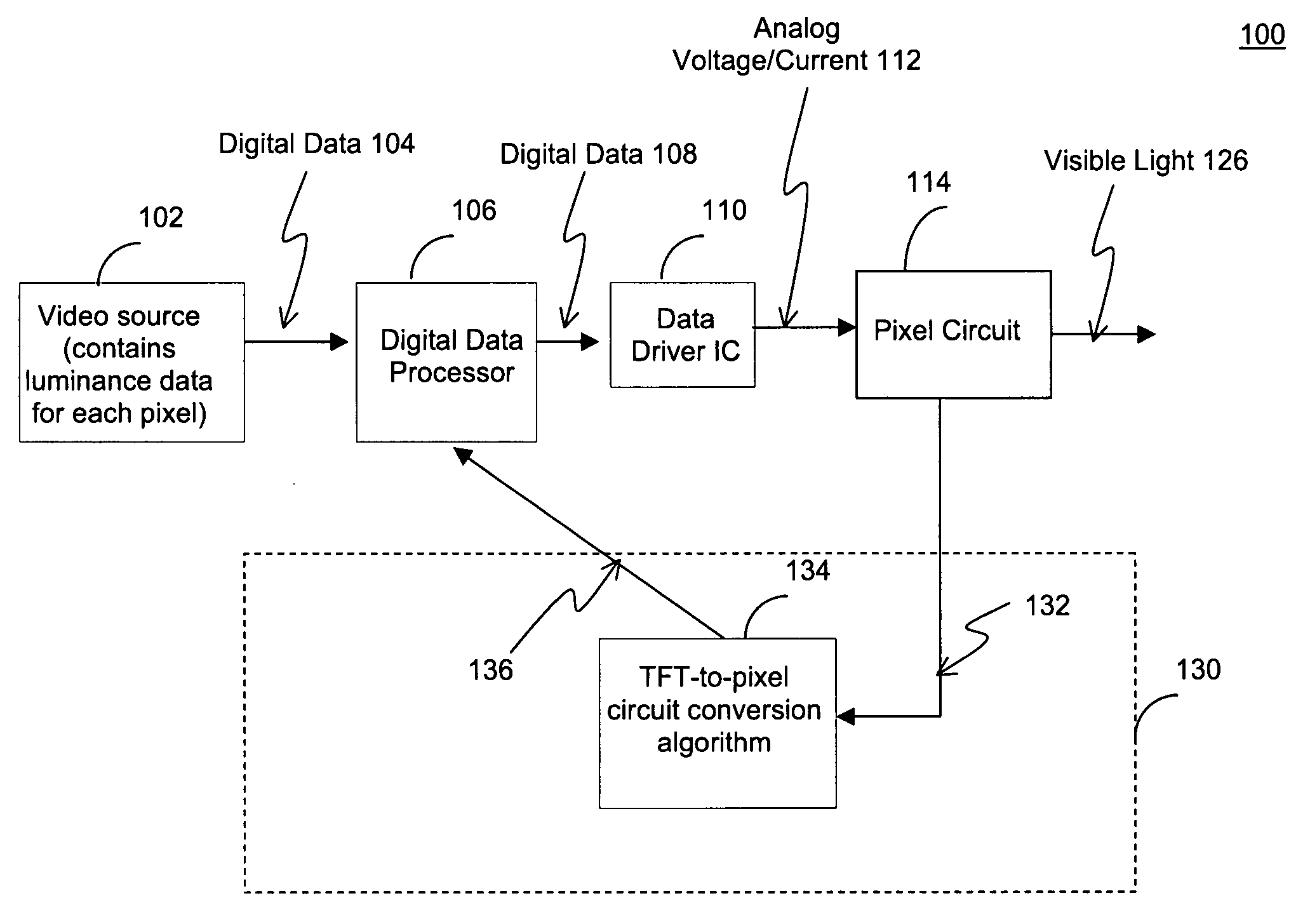
[0030]FIG. 3 illustrates the operation of a light emitting display system 100 to which a compensation scheme in accordance with an embodiment of the present invention is applied. A video source 102 contains luminance data for each pixel and sends the luminance data in the form of digital data 104 to a digital data processor 106. The digital data processor 16 may perform som...


PUM


Abstract

A method and system for compensation of non-uniformities in light emitting device displays is provided. The system includes a module for estimating degradation of an entire pixel circuit based on measurement of a part of the pixel circuit. Based on the estimation, a correction factor is produced to correct non-uniformity of the display.

Description

FIELD OF INVENTION [0001] The present invention relates to display technologies, more specifically a method and system for compensating for non-uniformities of elements in light emitting device displays. BACKGROUND OF THE INVENTION [0002] Active-Matrix Organic Light-Emitting Diode (AMOLED) displays are well known art. Amorphous silicon is, for example, one of promising materials for the AMOLED displays, due to its low cost and vast installed infrastructure from TFT-LCD fabrication. [0003] All AMOLED displays, regardless of backplane technology used, exhibit differences in luminance on a pixel to pixel basis, primarily as a result of process or construction inequalities, or from aging caused by operational use over time. Luminance non-uniformities in a display may also arise from natural differences in chemistry and performance from the OLED materials themselves. These non-uniformities must be managed by the AMOLED display electronics in order for the display device to attain commerc...

Claims


Application Information

Patent Timeline
Patent Type & Authority Applications(United States)
IPC IPC(8): G09G3/30G09G3/3225
CPCG09G3/3241G09G2300/0842G09G2320/0285G09G5/10G09G2320/0295G09G2320/043G09G2320/045G09G2320/029G09G3/30G01R19/00G09G3/20G09G3/32
Inventor NATHAN, AROKIAALEXANDER, STEFANSERVATI, PEYMANCHAJI, G. REZAHUANG, RICK I-HENGCHURCH, CORBIN
Owner IGNIS INNOVATION
Why Eureka
Try Eureka