Image forming apparatus
a technology of image forming apparatus and forming tube, which is applied in the direction of instruments, discharge tube luminescnet screens, electrographic processes, etc., can solve the problem that the existence does not easily exercise an influence on the trajectory of electron beams, and achieve the effect of suppressing cumulative charging, suppressing short charging time, and preventing deterioration of display characteristics
- Summary
- Abstract
- Description
- Claims
- Application Information
AI Technical Summary
Benefits of technology
Problems solved by technology
Method used
Image
Examples
example 1
[0070] The spacers which are used in the invention are manufactured as follows.
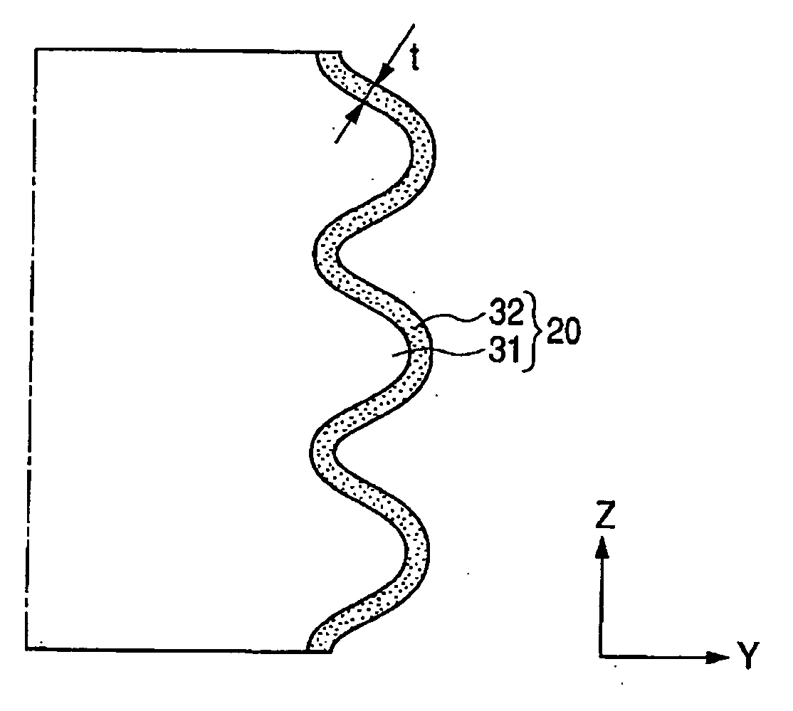
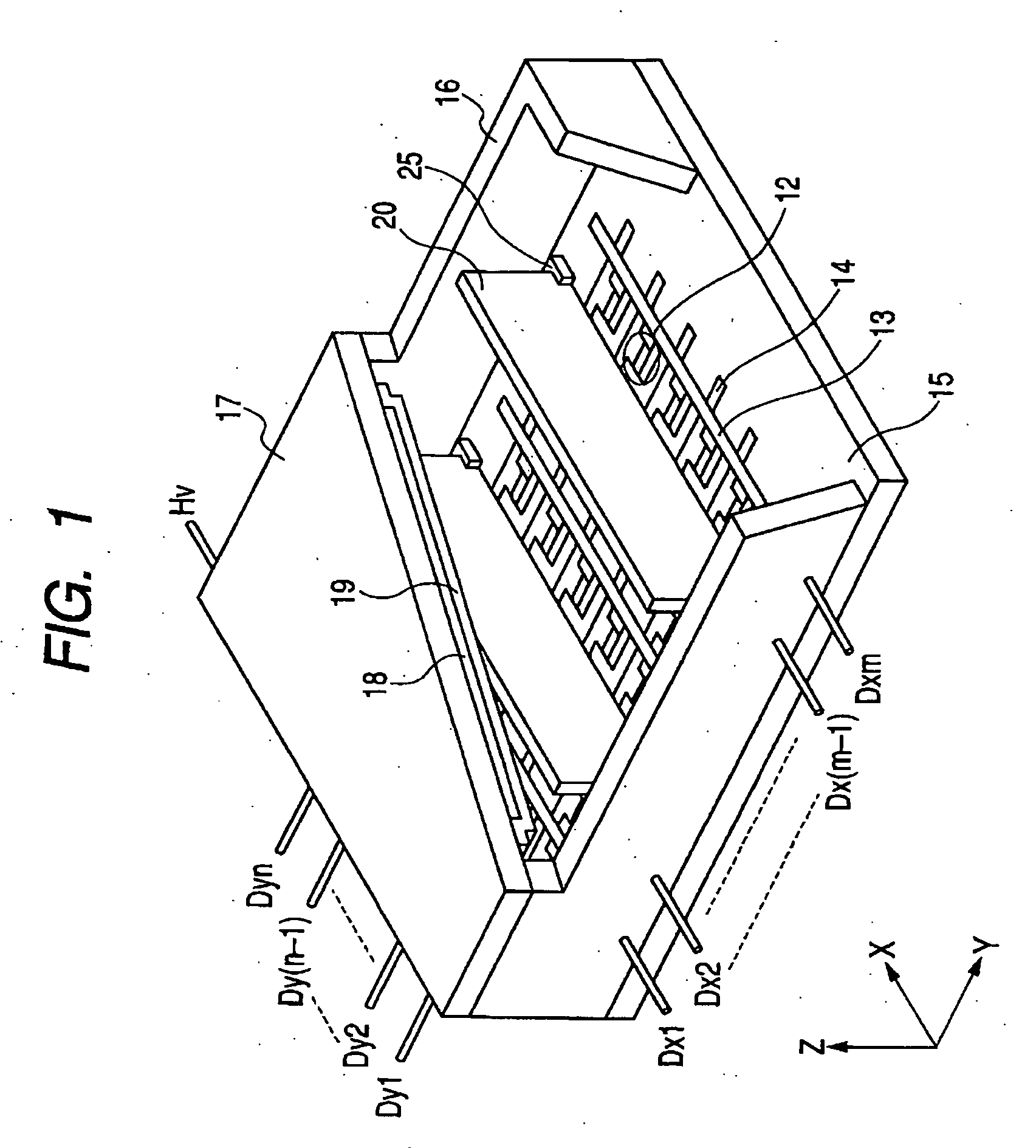
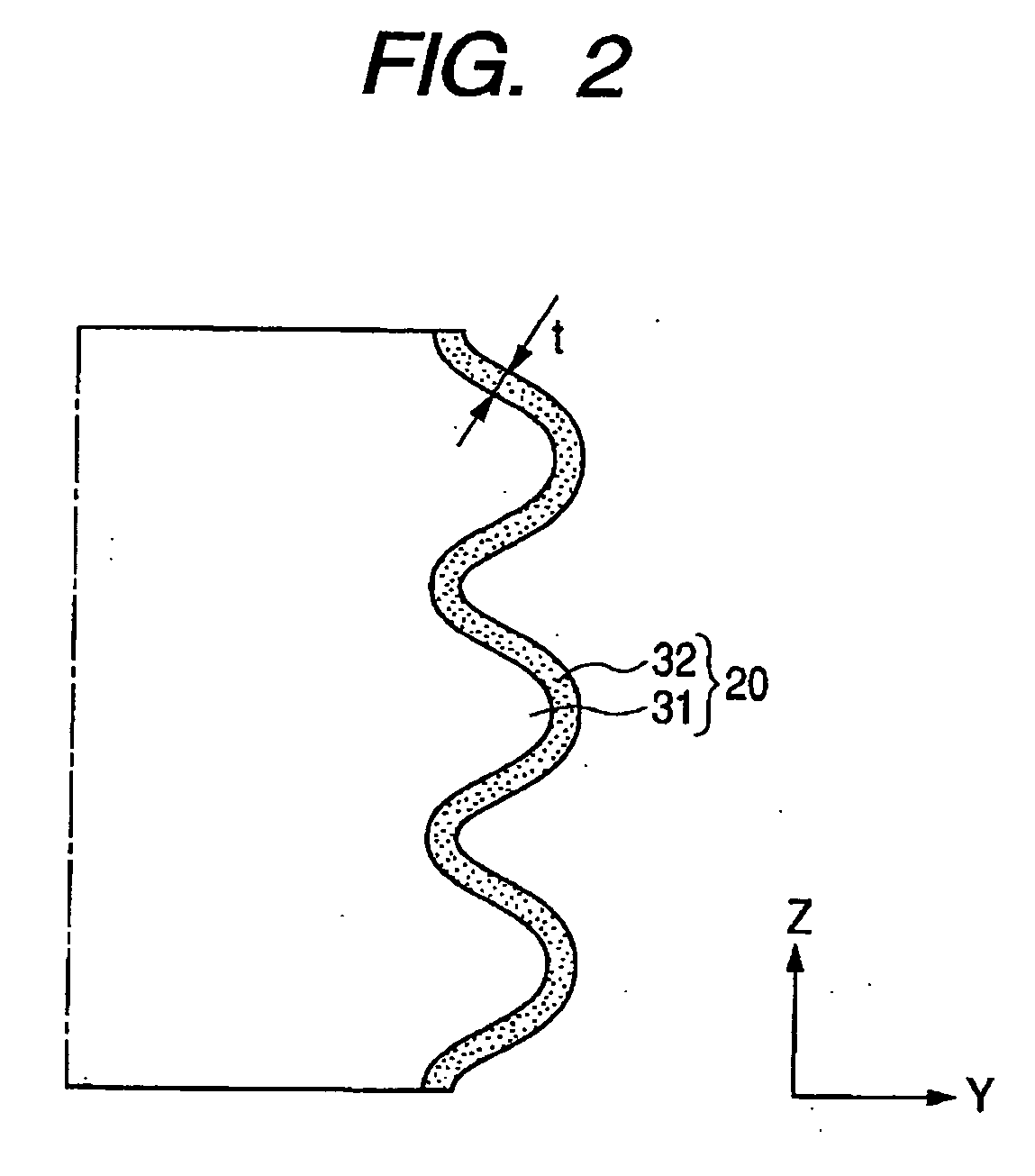
[0071] A substrate (PD200 made by Asahi Glass Co., Ltd.) is used as a base material and worked into a proper shape by a heat drawing method and a resultant plate is prepared as an insulating substrate of the spacer. The substrate has dimensions of (1.7 mm×0.18 mm×820 mm) and convex portions whose cross sectional shape is an almost trapezoid and whose average height is equal to 8 μm are formed at a pitch of 30 μm on the surface of (820 mm×1.7 mm) (hereinafter, referred to as a side surface). Surfaces of (0.18 mm×820 mm) (hereinafter, referred to as a contact surface) are formed in a flat shape so as to be come into contact with the cathode (upper wirings) and the anode (metal back). A corner between the side surface and the bottom surface is formed in a round shape so as to minimize the chipping and its radius of curvature is set to 5 μm. The concave and convex portions and the round shape of the corner p...
example 2
[0080] The spacer is formed and the image forming apparatus is constructed and driven in a manner similar to Example 1 except that the electrodes made of Pt are formed on the bottom surfaces (that is, two positions of the surfaces of 0.18 mm×820 mm) of the spacer. Thus, even if the apparatus is driven for a long time, a positional deviation of the electron beam near the spacer is not found. Further, it has been confirmed that, even in the depth region of the high resistance film on the spacer surface, the electric potential specification by the current field of the spacer is satisfied.
example 3
[0081] The spacer is formed and the image forming apparatus is constructed in a manner similar to Example 1 except that insulating layer (volume resistance at 25° C.: 3×10¹¹ Ωcm or more) of amorphous carbon is stacked and formed on the surface of the high resistance film so as to have a thickness of 10 nm. Thus, even if the apparatus is driven for a long time, a positional deviation of the electron beam near the spacer is not found. It has been confirmed that, even in the depth region of the high resistance film on the spacer surface, the electric potential specification by the current field of the spacer is satisfied.
[0082] A film density of the WGeN film of each of the high resistance films 2 of the spacers 1-1 and 1-4 in Example 1 is equal to 16 g / cm3 and a film density of the high resistance film 1 (PtAlN film) of the first layer is equal to 9.1 g / cm3. The film density is obtained by measuring the RBS:Rutherford Backscattering Spectrometory to determine the m value.
[0083] A me...
PUM
 Abstract
Description
Claims
Application Information
 - R&D
- Intellectual Property
- Life Sciences
- Materials
- Tech Scout
- Unparalleled Data Quality
- Higher Quality Content
- 60% Fewer Hallucinations
Browse by: Latest US Patents, China's latest patents, Technical Efficacy Thesaurus, Application Domain, Technology Topic, Popular Technical Reports.
© 2025 PatSnap. All rights reserved.Legal|Privacy policy|Modern Slavery Act Transparency Statement|Sitemap|About US| Contact US: help@patsnap.com


