
Contact probe for a testing head

a technology of contact probe and testing head, which is applied in the direction of electrical testing, measuring devices, instruments, etc., to achieve the effect of simple configuration

Active Publication Date: 2005-12-08
TECHNOPROBE
View PDF6 Cites 11 Cited by
  • Summary
  • Abstract
  • Description
  • Claims
  • Application Information

AI Technical Summary

Benefits of technology

The present invention provides a contact probe with a simple configuration that does not require deformation of the probe body for good electrical contact with an integrated electronic device. This allows for a reduction in the minimum distance between adjacent probes in a testing head and also the pitch of the contact pads of the tested devices. The contact probe has an eccentric contact tip positioned within the probe body contour. A testing head is also provided with vertical probes that ensure mechanical and electrical contact with a corresponding contact pad of the tested device. The contact probe is made by a method involving at least one cutting step of the tip portion along a plurality of cutting planes sloping with respect to a section plane. The technical effects of the invention include improved efficiency and accuracy in testing integrated electronic devices.

Problems solved by technology

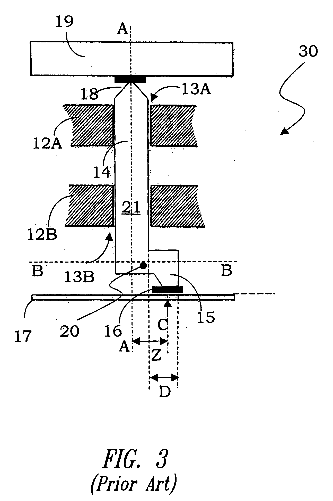
A very felt problem in the specific technical field is that of the reduction of the distance which separates the contact pads 8 of the device being tested, this distance being known in the field as “pitch”.

Method used


Image

  • Contact probe for a testing head
  • Contact probe for a testing head
  • Contact probe for a testing head

Examples


Embodiment Construction

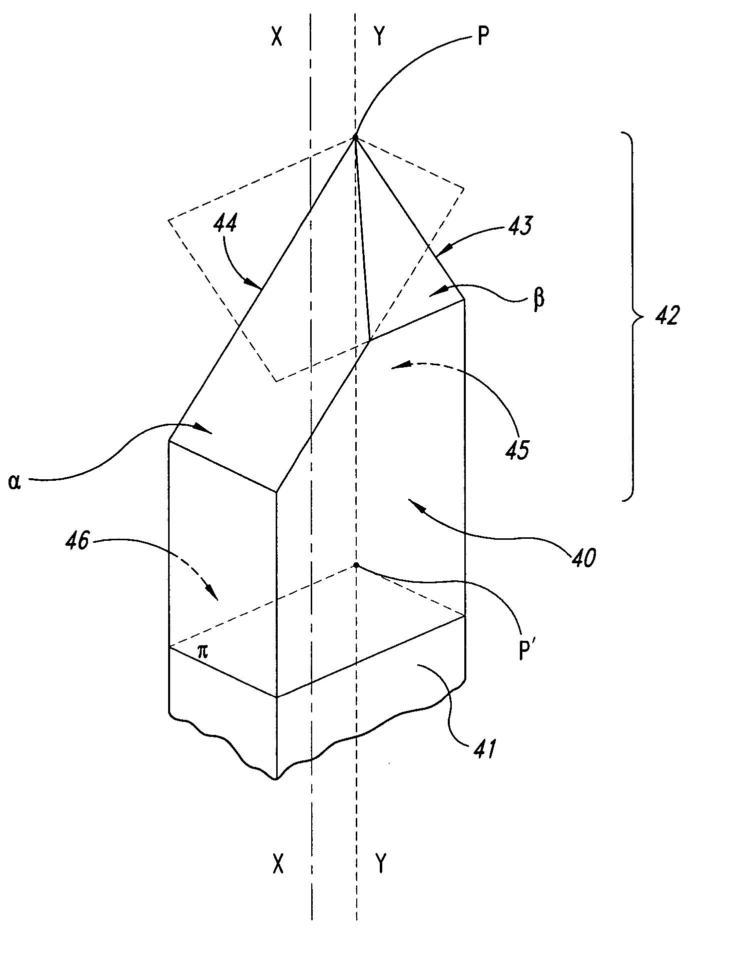
[0050] Making reference to FIG. 4A, 40 globally and schematically indicates a contact probe according to an embodiment of the invention.

[0051]FIG. 4B shows an enlarged view of the sole end or tip 42 portion of the probe, in correspondence with a contact tip P effective to put into contact a contact pad of a device to be tested (not shown).

[0052] As it has been seen with reference to the prior art, the contact probe 40 has a substantially rod-like probe body 41 having a central longitudinal axis XX and an overall contour. The probe 40 also includes a tip portion 42 extending from the probe body 41 and provided with an eccentric contact tip P.

[0053] Advantageously according to an embodiment of the invention, the contact tip P of the probe 40 is positioned within an extension of the contour of the probe body 41, as shown in FIG. 4B where the projection P′ of the contact tip P in correspondence with a section plane π has been indicated.

[0054] It is proper to underline that “contour”...


PUM


Abstract

A contact probe for a testing head effective to test a plurality of semiconductor-integrated electronic devices comprises a rod-like probe body having a cross section of prefixed contour and provided in correspondence with at least one end with an eccentric contact tip. The contact tip is positioned within the contour of the cross section of the probe body.

Description

BACKGROUND OF THE INVENTION [0001] 1. Field of the Invention [0002] The present invention relates to a contact probe for a testing head effective to test a plurality of semiconductor-integrated electronic devices comprising a plurality of so-called contact pads. [0003] The invention particularly, but not exclusively, relates to a testing head having vertical probes for testing semiconductor-integrated electronic devices and the following description is made with reference to this field of application for convenience of illustration only. [0004] 2. Description of the Related Art [0005] As it is well known, a testing head is essentially a device effective to electrically interconnect a plurality of contact pads of a semiconductor-integrated electronic device with corresponding channels of a testing machine which performs the test thereof. [0006] The test carried out on integrated electronic devices is effective to detect and isolate devices already faulty during the manufacturing step...

Claims


Application Information

Patent Timeline
Patent Type & Authority Applications(United States)
IPC IPC(8): G01R1/067G01R1/073
CPCG01R1/07314G01R1/06738G01R1/07357
Inventor CRIPPA, GIUSEPPEFELICI, STEFANO
Owner TECHNOPROBE
Learn More