Selecting a profile model for use in optical metrology using a machine learining system

Inactive Publication Date: 2005-09-01
TOKYO ELECTRON LTD
View PDF22 Cites 74 Cited by
  • Summary
  • Abstract
  • Description
  • Claims
  • Application Information

AI Technical Summary

Problems solved by technology

Calculating the model diffraction signal involves performing a large number of complex calculations, which can be time consuming and costly.

Method used


Image

  • Selecting a profile model for use in optical metrology using a machine learining system
  • Selecting a profile model for use in optical metrology using a machine learining system
  • Selecting a profile model for use in optical metrology using a machine learining system

Examples


Embodiment Construction

[0016] The following description sets forth numerous specific configurations, parameters, and the like. It should be recognized, however, that such description is not intended as a limitation on the scope of the present invention, but is instead provided as a description of exemplary embodiments.

1. Optical Metrology

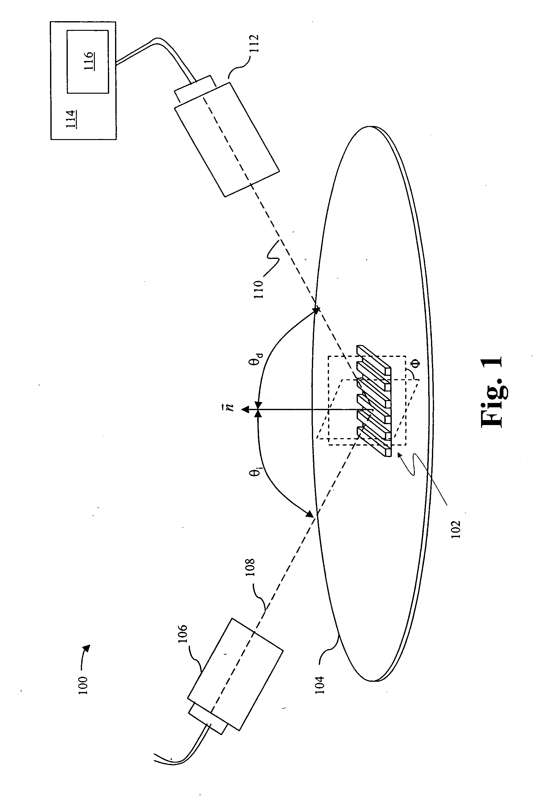
[0017] With reference to FIG. 1, an optical metrology system 100 can be used to examine and analyze a structure on a semiconductor wafer. For example, optical metrology system 100 can be used to determine a feature of a periodic grating 102 formed on wafer 104. As described earlier, periodic grating 102 can be formed in test areas on wafer 104, such as adjacent to a device formed on wafer 104. Alternatively, periodic grating 102 can be formed in an area of the device that does not interfere with the operation of the device or along scribe lines on wafer 104. Furthermore, in some applications, the device can be measured directly.

[0018] As depicted in FIG. 1, optical me...


PUM


Abstract

A profile model can be selected for use in examining a structure formed on a semiconductor wafer using optical metrology by obtaining an initial profile model having a set of profile parameters. A machine learning system is trained using the initial profile model. A simulated diffraction signal is generated for an optimized profile model using the trained machine learning system, where the optimized profile model has a set of profile parameters with the same or fewer profile parameters than the initial profile model. A determination is made as to whether the one or more termination criteria are met. If the one or more termination criteria are met, the optimized profile model is modified and another simulated diffraction signal is generated using the same trained machine learning system.

Description

BACKGROUND [0001] 1. Field of the Invention [0002] The present application relates to metrology of structures formed on semiconductor wafers, and more particularly to selecting a profile model for use in optical metrology using a machine learning system. [0003] 2. Related Art [0004] Optical metrology involves directing an incident beam at a structure, measuring the resulting diffracted beam, and analyzing the diffracted beam to determine a feature of the structure. In semiconductor manufacturing, optical metrology is typically used for quality assurance. For example, after fabricating a periodic grating in proximity to a semiconductor chip on a semiconductor wafer, an optical metrology system is used to determine the profile of the periodic grating. By determining the profile of the periodic grating, the quality of the fabrication process utilized to form the periodic grating, and by extension the semiconductor chip proximate the periodic grating, can be evaluated. [0005] One conven...

Claims


Application Information

Patent Timeline
IPC IPC(8): G06F15/18
CPCG06N99/005G03F7/70625G06N20/00
Inventor DREGE, EMMANUELDODDI, SRINIVASBAO, JUNWEI
Owner TOKYO ELECTRON LTD
Why Eureka
Try Eureka