
Microstrip band pass filter using end-coupled SIRs

a filter and microstrip technology, applied in the field of microstrip filters, can solve the problems of difficult to have good attenuation and narrowband characteristics, and unsuitable for millimeter wave bands, and achieve good attenuation characteristics

Inactive Publication Date: 2005-06-30
ELECTRONICS & TELECOMM RES INST
View PDF5 Cites 29 Cited by
  • Summary
  • Abstract
  • Description
  • Claims
  • Application Information

AI Technical Summary

Benefits of technology

The present invention is about a microstrip band pass filter that has good attenuation and narrowband characteristics, and is insensitive to manufacturing errors. It can make a fine frequency transition without distortion of the filter characteristics just by adjusting the width of the low impedance line. The invention also extracts a parasitic component value due to the discontinuous structure of the SIR and uses it to increase or reduce the length of the resonator for compensation, making it applicable for various frequency ranges with improved design accuracy. The microstrip band pass filter comprises a dielectric substrate, a conductor plate, and input and output terminals located on the substrate. The input and output terminals are conductors and end-coupled through gaps.

Problems solved by technology

Further, since a capacitance of the coupling line is changed together with an even mode impedance and an odd mode impedance according to the gap, it is sensitive to the manufacturing process error and it is difficult to have good attenuation and narrowband characteristics.
Therefore, the conventional planar type filters using the SIR are required to have the good attenuation and narrowband characteristics, and as the filter structures becomes smaller proportional to a wavelength, there occurs a problem that it is not suitable for use in the millimeter wave band (30 GHz to 300 GHz) that requires an insensitive characteristic to the small manufacturing process error.

Method used


Image

  • Microstrip band pass filter using end-coupled SIRs
  • Microstrip band pass filter using end-coupled SIRs
  • Microstrip band pass filter using end-coupled SIRs

Examples


Embodiment Construction

[0019] The present invention will now be described more fully hereinafter with reference to the accompanying drawings, in which preferred embodiments of the invention are shown. This invention may, however, be embodied in different forms and should not be construed as limited to the embodiments set forth herein. Rather, these embodiments are provided so that this disclosure will be thorough and complete, and will fully convey the scope of the invention to those skilled in the art.

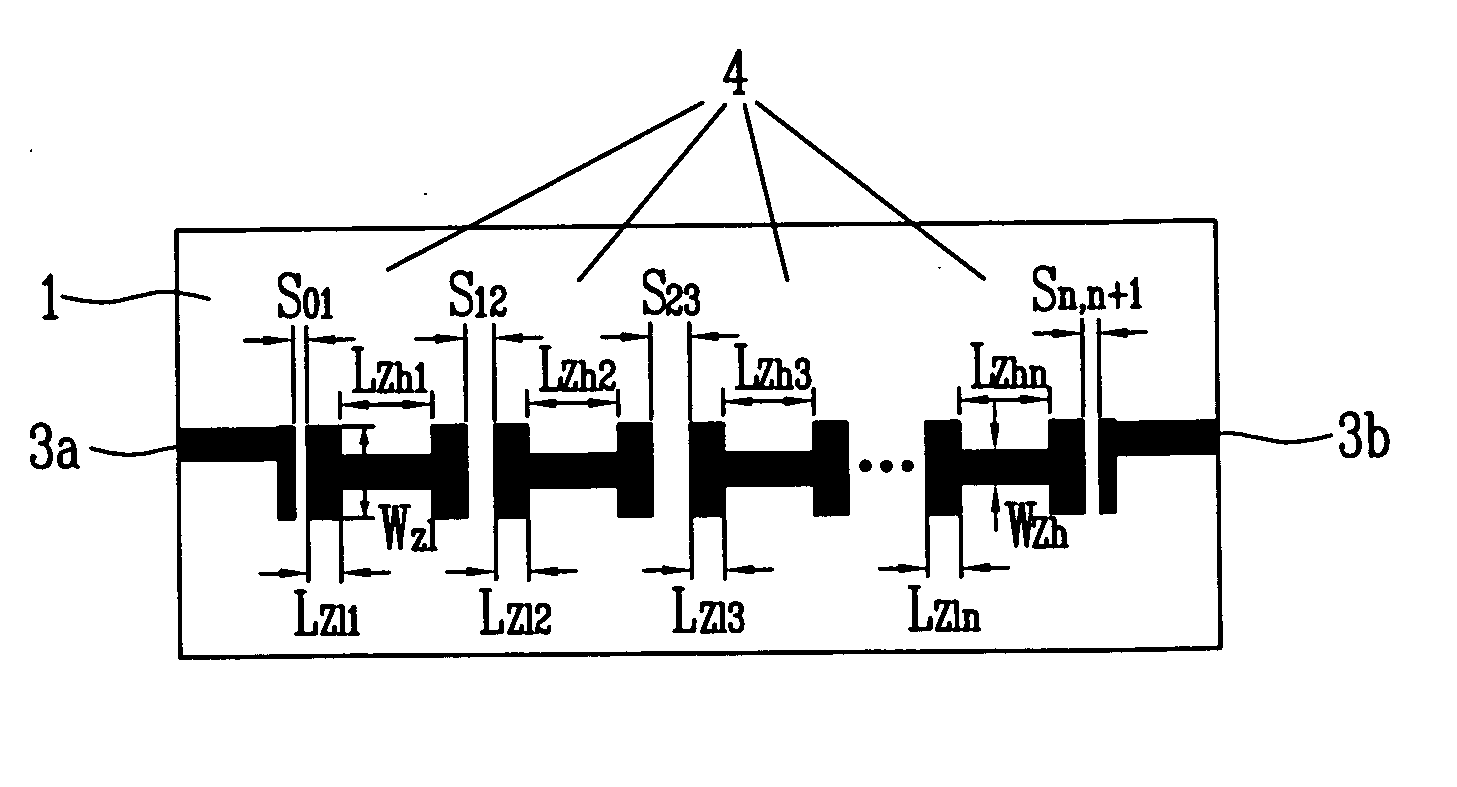
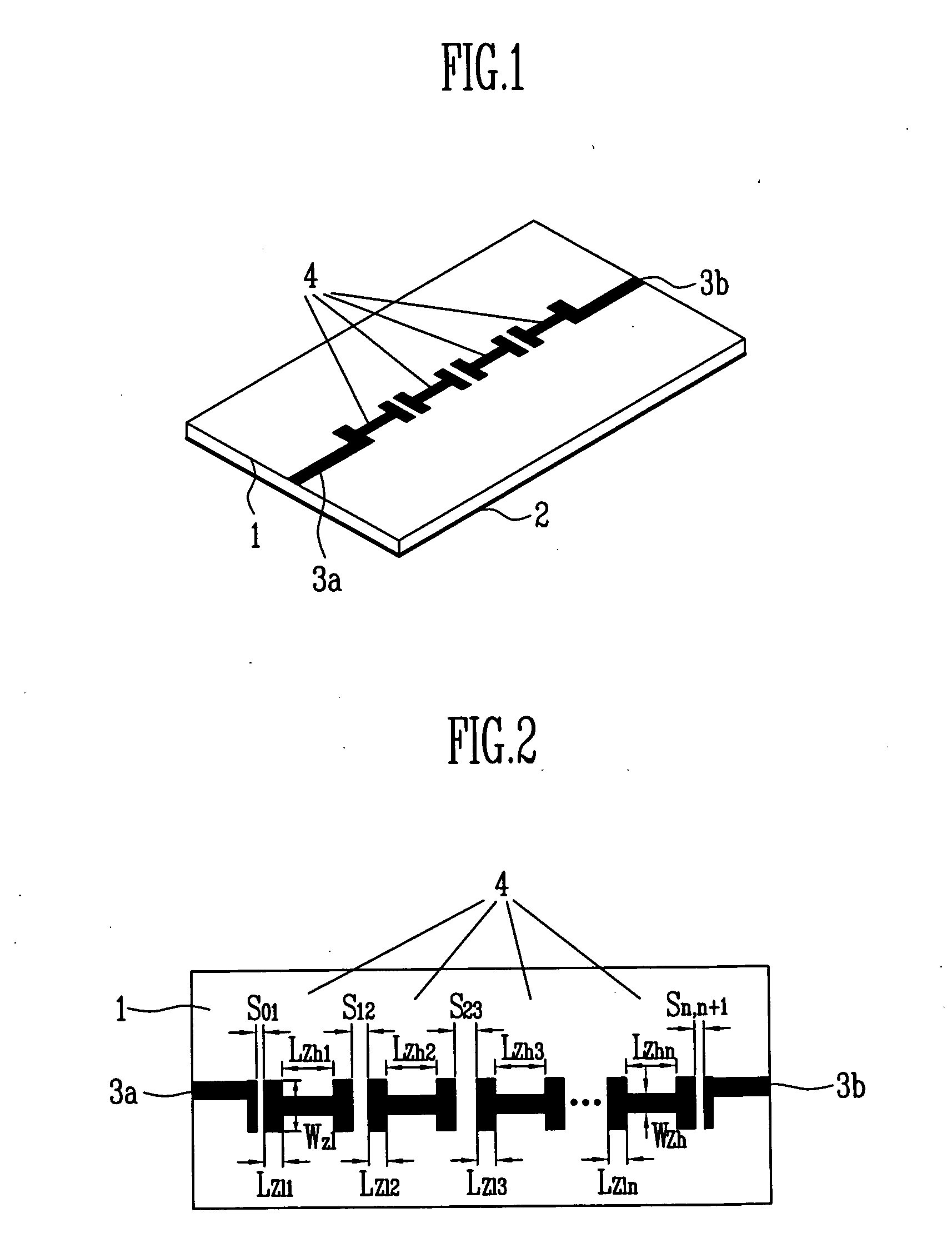
[0020]FIG. 1 is a structural diagram of a microstrip band pass filter according to a first embodiment of the present invention. In FIG. 1, the microstrip band pass filter comprises a dielectric substrate 1, a conductive plate 2 arranged on a lower surface of the dielectric substrate, input and output terminals 3a, 3b located on an upper surface of the dielectric substrate in series and made of a conductor, and a plurality of SIRs 4. That is, the conductive input and output terminals 3a, 3b and the pluralit...


PUM


Abstract

The present invention relates to a microstrip band pass filter and, more specifically, to a microstrip band pass filter using end-coupled stepped impedance resonators that can be used in a millimeter wave band, wherein the microstrip band pass filter comprises: a dielectric substrate; a conductor plate located on a lower surface of the dielectric substrate; and an input terminal, a plurality of SIRs and an output terminal located on an upper surface of the dielectric substrate in series, wherein the input terminal, the plurality of SIRs and the outputs terminal are conductors and end-coupled through gaps, whereby the microstrip band pass filter has a good attenuation characteristic and a narrowband characteristic, and is insensitive to the manufacturing error, and a fine frequency transition can be made without distortion just with width adjustment of the low impedance transmission line of the SIR.

Description

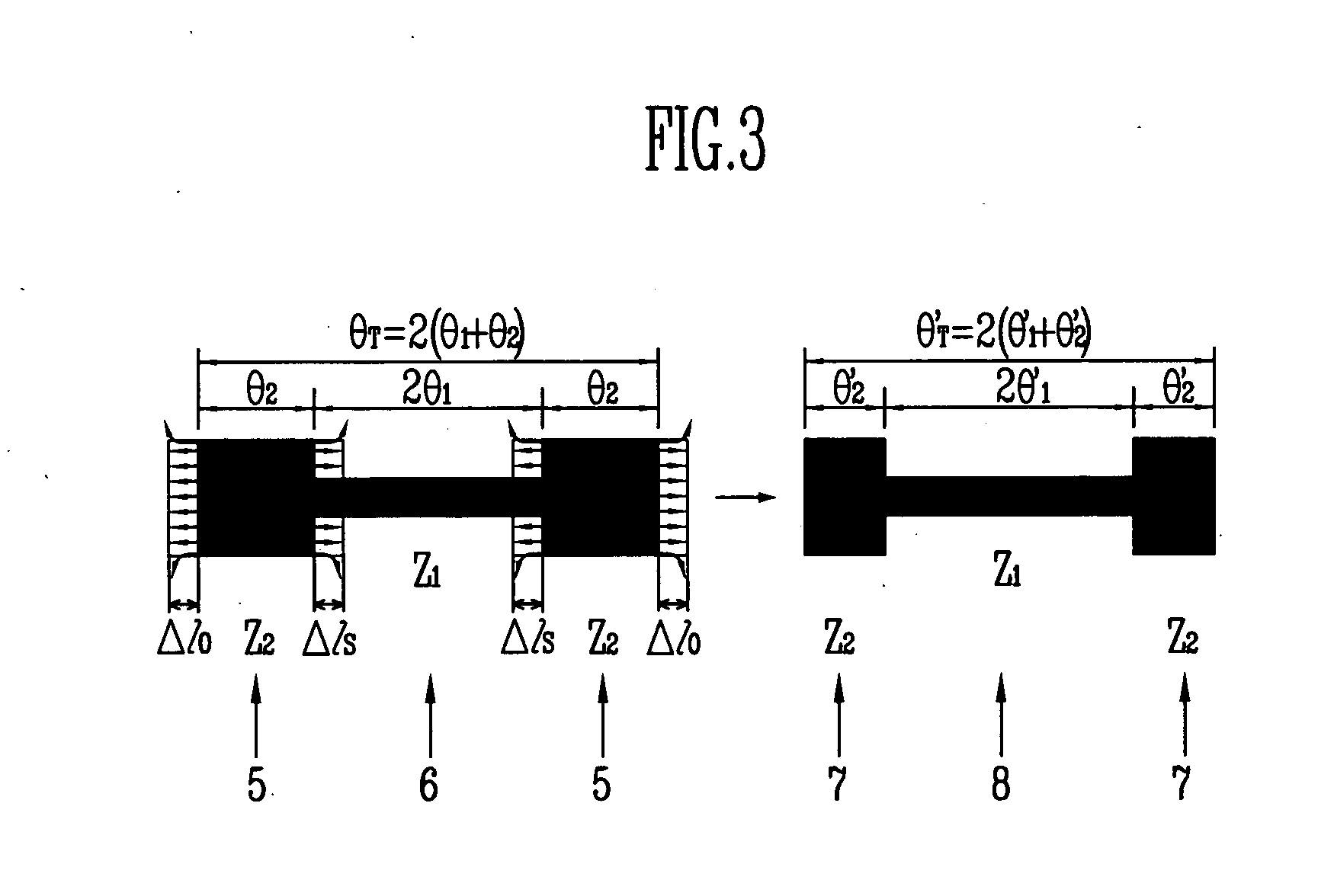
BACKGROUND [0001] 1. Field of the Invention [0002] The present invention generally relates to a microstrip band pass filter. More specifically, the present invention relates to a microstrip band pass filter using end-coupled stepped impedance resonators (hereinafter, referred to as “SIR”) that can be used in a millimeter wave band. [0003] 2. Discussion of Related Art [0004] A microstrip line represents a transmission line that has a pair of conductive thin films at both sides and a dielectric substrate therebetween. It is also referred to as “microstrip transmission line”. The upper conductor has a designated shape (strip type) and the lower conductor is formed of a wide ground conductor. Further, there can exist an up-down symmetrical structure where another dielectric is located on the upper conductor. The SIR is a resonator that transmits a signal in a specific frequency band and blocks signals in other frequency bands based on the impedance ratio and length of the microstrip lin...

Claims


Application Information

Patent Timeline
Patent Type & Authority Applications(United States)
IPC IPC(8): H01P1/203
CPCH01P1/20381H01P1/203
Inventor KO, KYOUNG SUKJUN, DONG SUKKIM, DONG YOUNGLEE, HONG YEOLLEE, SANG SEOK
Owner ELECTRONICS & TELECOMM RES INST
Learn More