Method for manufacturing Semiconductor device, adhesive sheet for use therein and semiconductor device
a technology of adhesive sheets and semiconductor devices, which is applied in the direction of semiconductor devices, semiconductor/solid-state device details, electrical apparatus, etc., can solve the problems that the material of the base member b>3/b> such as fluoropolymer, silicone, and fluoro-coated metals as disclosed in the publication can never meet the above contrary requirements for contact, and achieves less cracking or chipping of the semiconductor element, thinning the semiconductor device, and cost reduction
- Summary
- Abstract
- Description
- Claims
- Application Information
AI Technical Summary
Benefits of technology
Problems solved by technology
Method used
Image

Examples
example 1
[0076] Production of Adhesive Sheet
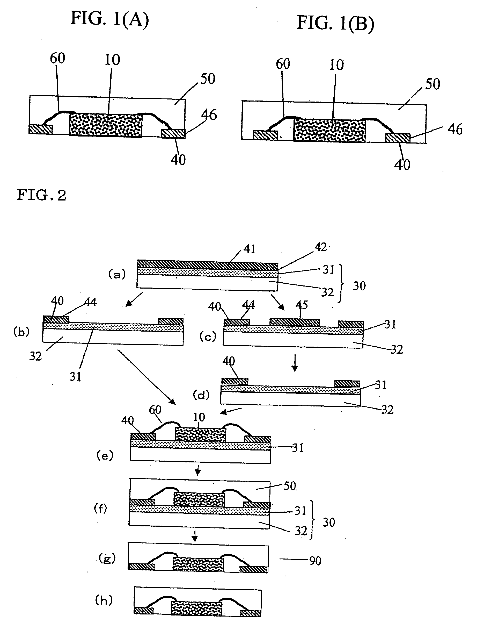
[0077] A silicone-based adhesive (SD-4587L, Toray Dow Corning Co., Ltd.) was applied onto a polyimide film with a thickness of 25 μm and a width of 500 mm (Kapton® H, Du Pont-Toray Co., Ltd.) and then dried at 150° C. for 3 minutes to form an adhesive sheet having an adhesive layer with a thickness of 5 μm. The adhesive layer of the adhesive sheet had an elastic modulus of 0.15 MPa at 150° C. and an adhesive strength of 0.25 N / 10 mm to a silicon mirror wafer. The polyimide film used as the base layer had an elastic modulus of 1.8 GPa at 150° C.
[0078] Fabrication of Semiconductor Device
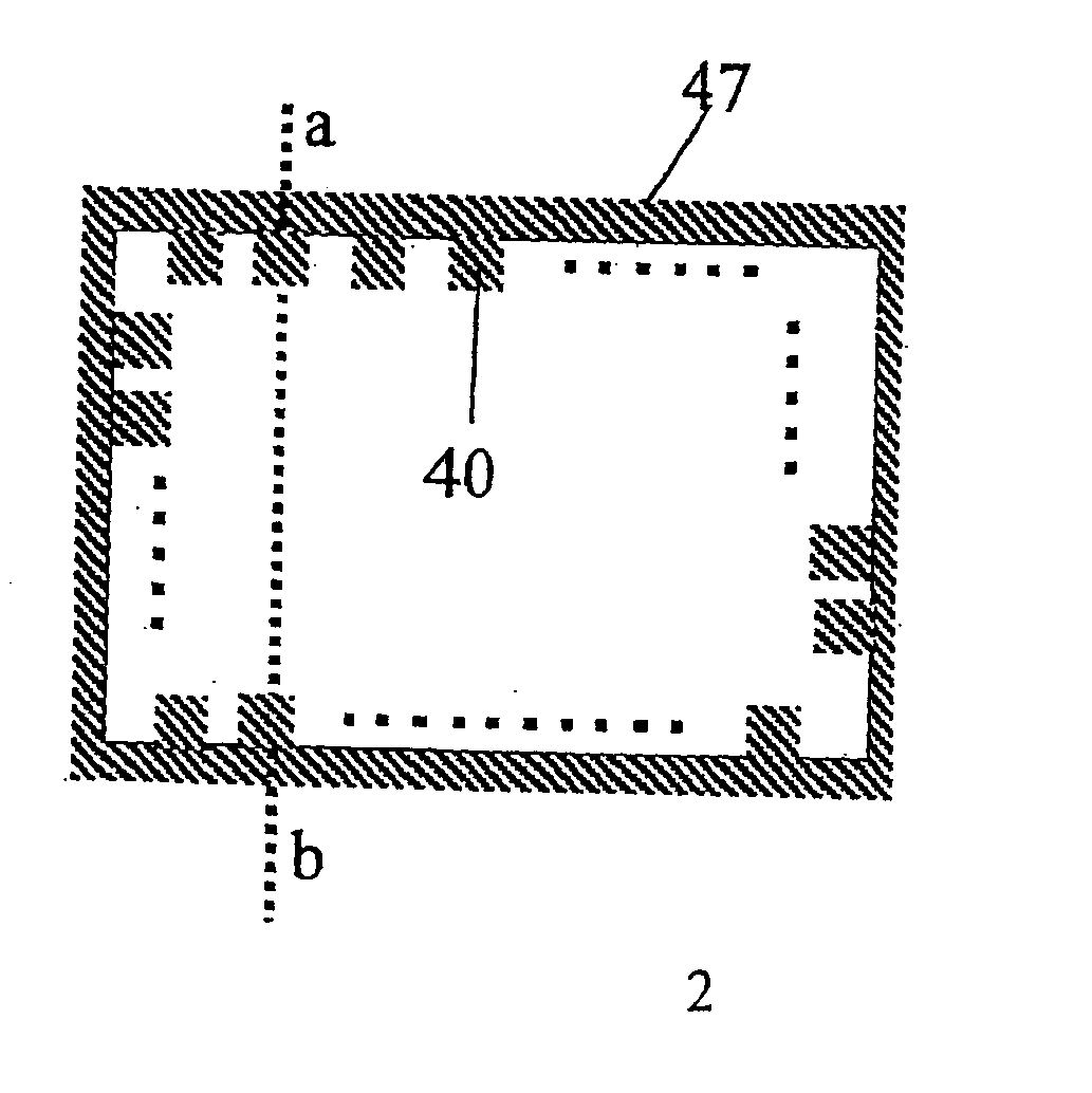
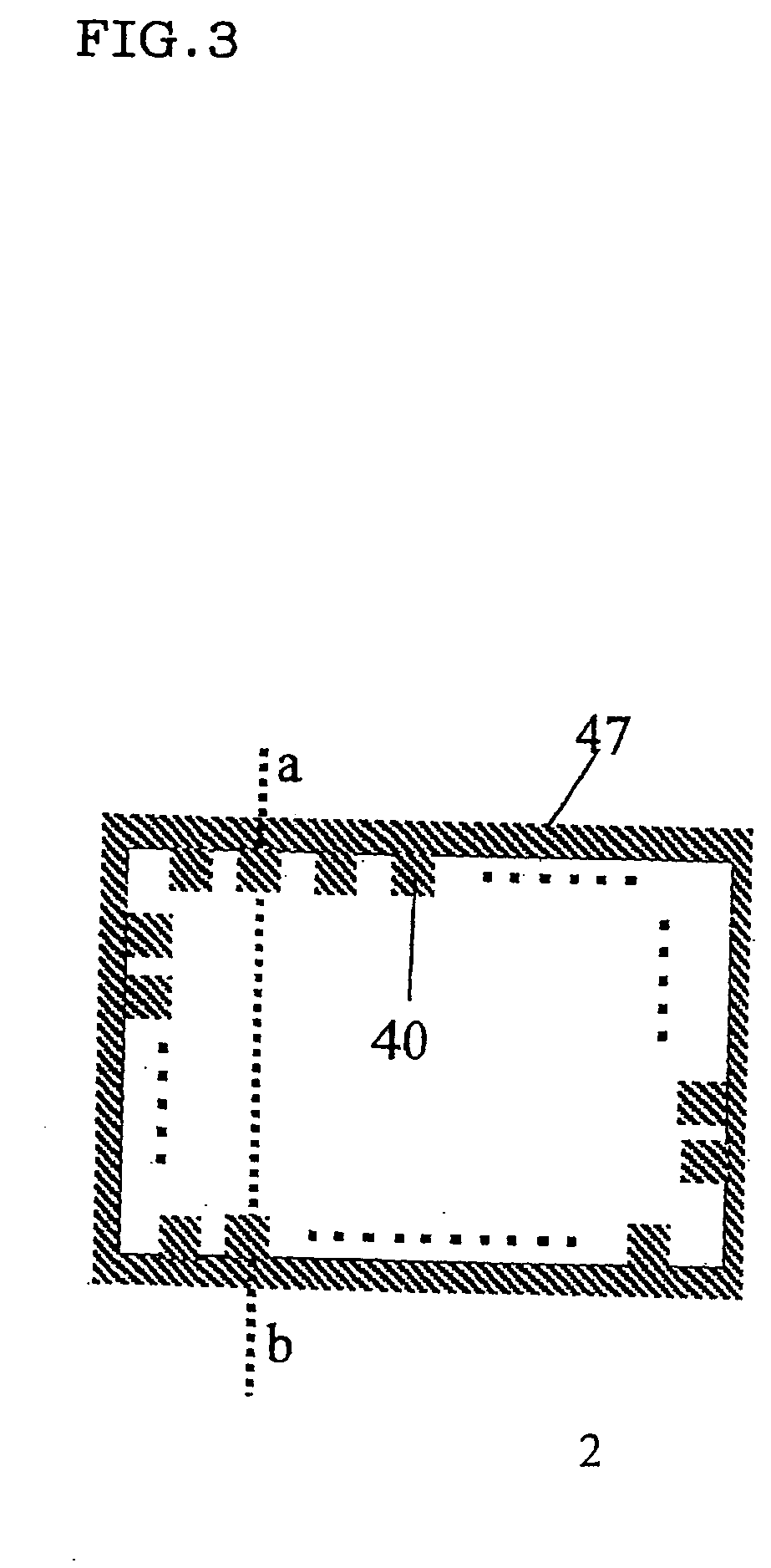
[0079] A copper metal foil with a thickness of 35 μm (BHY-138T, Japan Energy Corporation) was attached to the adhesive layer of the adhesive sheet to form a flexible metal-attached adhesive sheet. After pattern etching, one block corresponding to each block 80 (with a W1 of 500 mm) as shown in FIG. 5 had an arrangement of the electrically conductive parts 40 as sho...
example 2
[0083] The process of Example 1 was used to form semiconductor devices except that the metal foil used was a copper-nickel alloy foil with a thickness of 18 μm (C7025, Japan Energy Corporation). The wire bonding had a 100% success rate. The observation of the inside of the resulting semiconductor devices proved that they had no deformed wire, no shifted chip, or the like.
Wire Bonding Conditions
[0084] Apparatus: UTC-300BI SUPER (Shinkawa Ltd.)
[0085] Ultrasonic Frequency: 115 kHz
[0086] Ultrasonic Output Time: 15 milliseconds
[0087] Ultrasonic Output Power: 120 mW
[0088] Bond Load: 1.18 N
[0089] Search Load: 1.37 N
Transfer Molding Conditions
[0090] Apparatus: TOWA Molding Machine
[0091] Molding Temperature: 175° C.
[0092] Time: 90 seconds
[0093] Clamp Pressure: 200 kN
[0094] Transfer Speed: 3 mm / second
[0095] Transfer Pressure: 5 kN
Elastic Modulus Determining Method
[0096] The elastic modulus of the base layer and the adhesive layer were measured under the following conditions...
PUM
 Abstract
Description
Claims
Application Information
 - R&D
- Intellectual Property
- Life Sciences
- Materials
- Tech Scout
- Unparalleled Data Quality
- Higher Quality Content
- 60% Fewer Hallucinations
Browse by: Latest US Patents, China's latest patents, Technical Efficacy Thesaurus, Application Domain, Technology Topic, Popular Technical Reports.
© 2025 PatSnap. All rights reserved.Legal|Privacy policy|Modern Slavery Act Transparency Statement|Sitemap|About US| Contact US: help@patsnap.com