
Integrated circuits, and design and manufacture thereof

a technology of integrated circuits and circuits, applied in the field of integrated circuits, can solve the problems of significant commercial and technical gap between asic and fpga technology, circuit faults in asics can be difficult and expensive to correct, and design asics are expensive and time-consuming, so as to reduce or avoid leakage currents, and improve the degree of cell reusability

Inactive Publication Date: 2005-06-02
LSI CORPORATION
View PDF10 Cites 14 Cited by
  • Summary
  • Abstract
  • Description
  • Claims
  • Application Information

AI Technical Summary

Benefits of technology

[0005] Advantages, features and objects of the invention may include: (i) enabling cells of a module that is not selected for use, to be available as reusable resources; (ii) providing a module architecture to enable cells to be reused if the module is not selected for use; (iii) enabling control of which cells of a module are available for re-use if the module is not selected for use; (iv) providing different representations of a module with different degrees of cell reusability; (v) enabling efficient routing of a connection wire directly over a module that is not selected for use; (vi) reducing or avoiding leakage currents associated with cells of unused modules; and / or (v) extending a versatility of an integrated circuit by distributing sub-circuits within a general-purpose area of the integrated circuit. Other features, objects and advantages of the invention will become apparent from the following description, claims and / or drawings.

Problems solved by technology

However, there is significant commercial and technical gap between ASIC and FPGA technologies.
An ASIC can offer optimum performance, but designing an ASIC is expensive and time-consuming.
Circuit faults in ASICS can also be difficult and expensive to correct.
An ASIC is also expensive to manufacture if in small volumes.
Although generally less expensive than an ASIC, an FPGA does not contain dedicated circuitry, and is less optimized than an ASIC.
An FPGA has a certain amount of circuit overhead to facilitate the programmability of the FPGA, and is not useable as part of the custom circuit.

Method used


Image

  • Integrated circuits, and design and manufacture thereof
  • Integrated circuits, and design and manufacture thereof
  • Integrated circuits, and design and manufacture thereof

Examples


Embodiment Construction

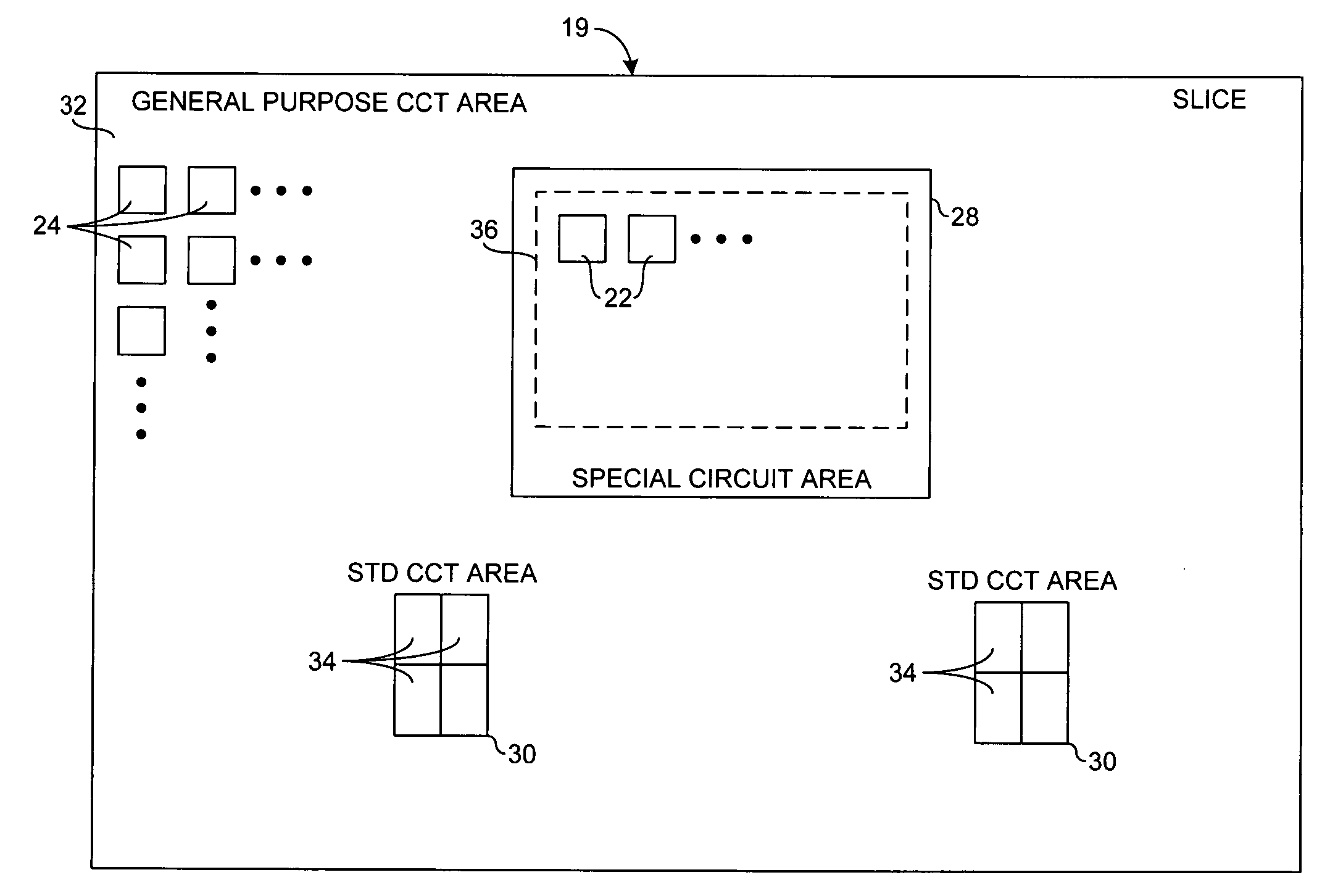
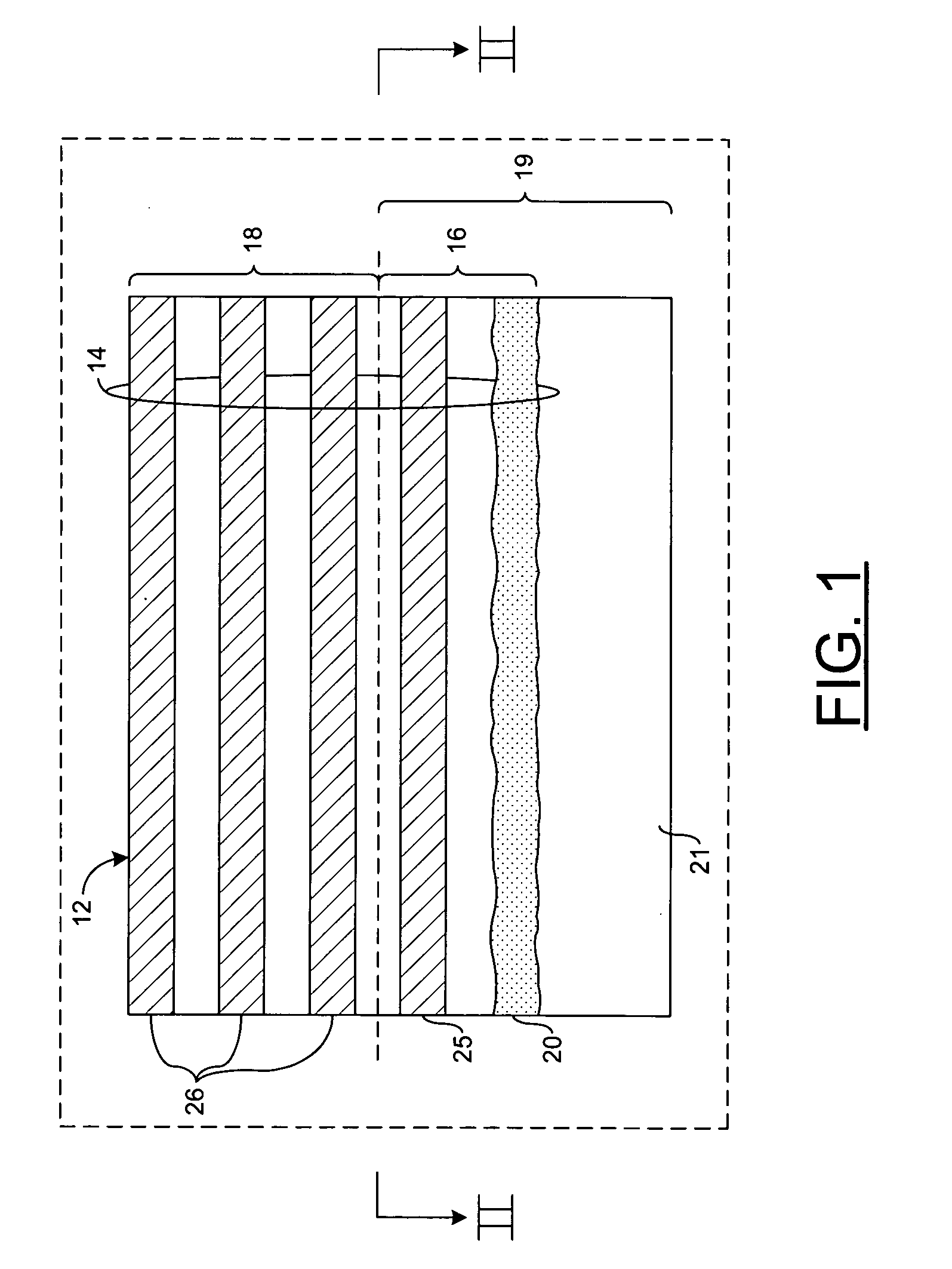
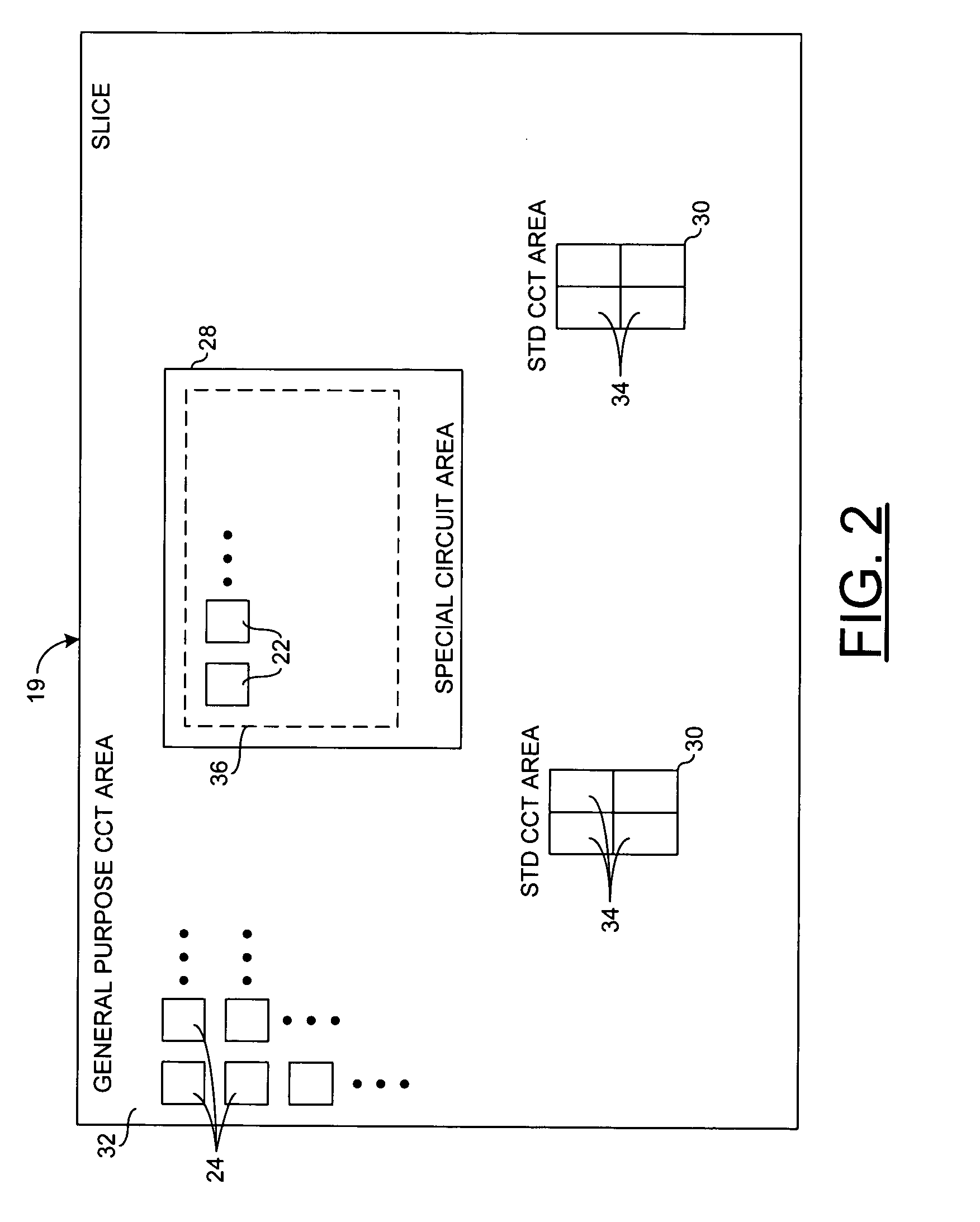
[0021] Referring to FIGS. 1 and 2, an integrated circuit (IC) 10 is shown. The IC may comprise a die 12 within which a circuit 14 may be implemented. The circuit 14 may be, in one example, a logic circuit. The circuit 14 may be a custom circuit for a dedicated circuit application. The die 12 may include one or more patterned custom-independent layers 16 and one or more patterned custom-specific layers 18 (for the sake of clarity, the patterning is not shown in FIG. 1). The custom-independent layers 16 may be referred to as base layers. The custom independent layers 16 may be pre-designed for a certain general type of circuit application prior to customization. Customization for a specific circuit application may be provided by the custom-specific layers 18. Different dies 12 with different customizations (e.g., different custom-specific layers 18) may include the same custom-independent layers 16.

[0022] A portion of the die 12 including only the custom-independent layers 16 may be ...


PUM


Abstract

An integrated circuit comprising a die having a surface. The die may comprise first and second areas. The first area may comprise first circuit cells. The first circuit cells may be configurable by user defined interconnections from above the surface. The second area may comprise a plurality of sub-circuit cells. The sub-circuit cells may form a module having a predefined functionality. The sub-circuit cells may include at least one second circuit cell. The second circuit cell may be configured such that when the predefined functionality of the module is not used, the second circuit cell is configurable by user defined interconnections from above the surface.

Description

FIELD OF THE INVENTION [0001] The present invention may relate generally to the field of integrated circuits, and the design and manufacture thereof. In one aspect, the invention may relate to a design technique in which a custom integrated circuit may be designed based on a predefined layout of integrated circuit elements. BACKGROUND TO THE INVENTION [0002] Application Specific Integrated Circuits (ASICs) and Field Programmable Gate Arrays (FPGAs) provide different technologies for implementing a custom integrated circuit. However, there is significant commercial and technical gap between ASIC and FPGA technologies. An ASIC is custom designed for a specific circuit application. An ASIC can offer optimum performance, but designing an ASIC is expensive and time-consuming. Circuit faults in ASICS can also be difficult and expensive to correct. An ASIC is also expensive to manufacture if in small volumes. An FPGA is a general purpose array of logic gates that can be configured as a cus...

Claims


Application Information

Patent Timeline
Patent Type & Authority Applications(United States)
IPC IPC(8): G06F17/50H01L27/02H01L27/118
CPCG06F17/5054H01L27/11803H01L27/0203G06F17/5068G06F30/34G06F2115/06G06F30/39G06F30/347
Inventor AURACHER, STEFANPRIBBERNOW, CLAUSHILS, ANDREAS
Owner LSI CORPORATION
Learn More