
Method of measuring threshold voltage for a NAND flash memory device

a threshold voltage and memory device technology, applied in electronic circuit testing, digital storage, instruments, etc., can solve the problems of inability of wordline drivers to transfer negative voltages to wordlines, and high difficulty in obtaining distribution profiles of threshold voltages of erased memory cells

Active Publication Date: 2005-05-19
STMICROELECTRONICS SRL +1
View PDF3 Cites 62 Cited by
  • Summary
  • Abstract
  • Description
  • Claims
  • Application Information

AI Technical Summary

Benefits of technology

The present invention provides a method for measuring the distribution profiles of negative threshold voltages in a NAND flash memory device. This method involves applying a voltage over 0V to a wordline of a memory cell instead of a negative voltage and establishing a gate-to-source voltage of the memory cell on a negative voltage by raising the voltages of drain, source, and well of the memory cell. The method allows for the measurement of threshold voltages in a NAND flash memory device with a plurality of cell strings, common drain nodes, common source nodes, wordlines, and a well of a semiconductor substrate. The method can detect voltage variations during a read operation and identify the threshold voltage of a selected memory cell based on the voltage variation. The technical effect of this invention is to provide a more accurate and efficient method for measuring threshold voltages in a NAND flash memory device.

Problems solved by technology

However, the wordline drivers are incapable of transferring negative voltages to the wordlines.
Therefore, as it is just available to use only positive voltages with the wordline drivers, there are high difficulties to obtain distribution profiles of threshold voltages of erased memory cells.

Method used


Image

  • Method of measuring threshold voltage for a NAND flash memory device
  • Method of measuring threshold voltage for a NAND flash memory device
  • Method of measuring threshold voltage for a NAND flash memory device

Examples


Embodiment Construction

[0016] Preferred embodiments of the present invention will be described below in more detail with reference to the accompanying drawings. The present invention may, however, be embodied in different forms and should not be constructed as limited to the embodiments set forth herein. Rather, these embodiments are provided so that this disclosure will be thorough and complete, and will fully convey the scope of the invention to those skilled in the art. Like numerals refer to like elements throughout the specification.

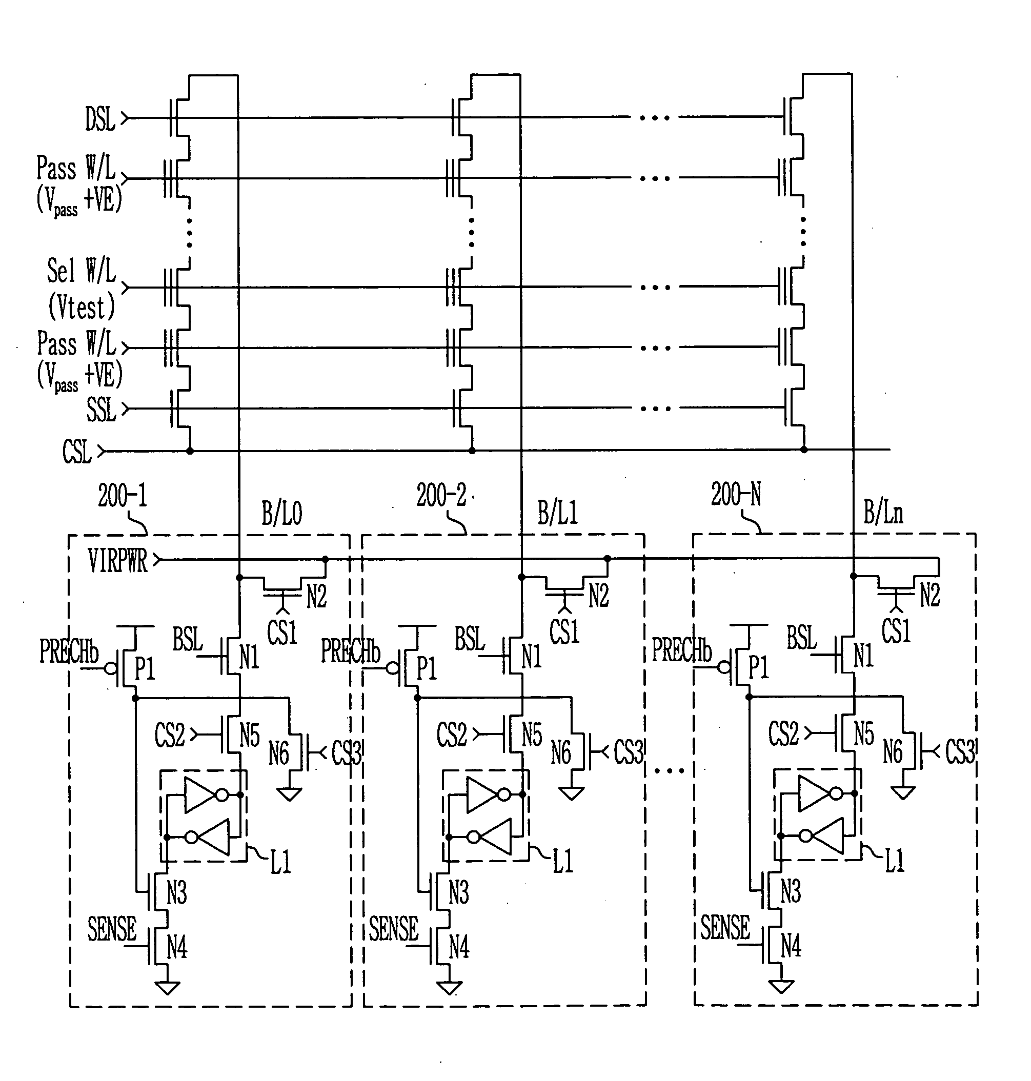
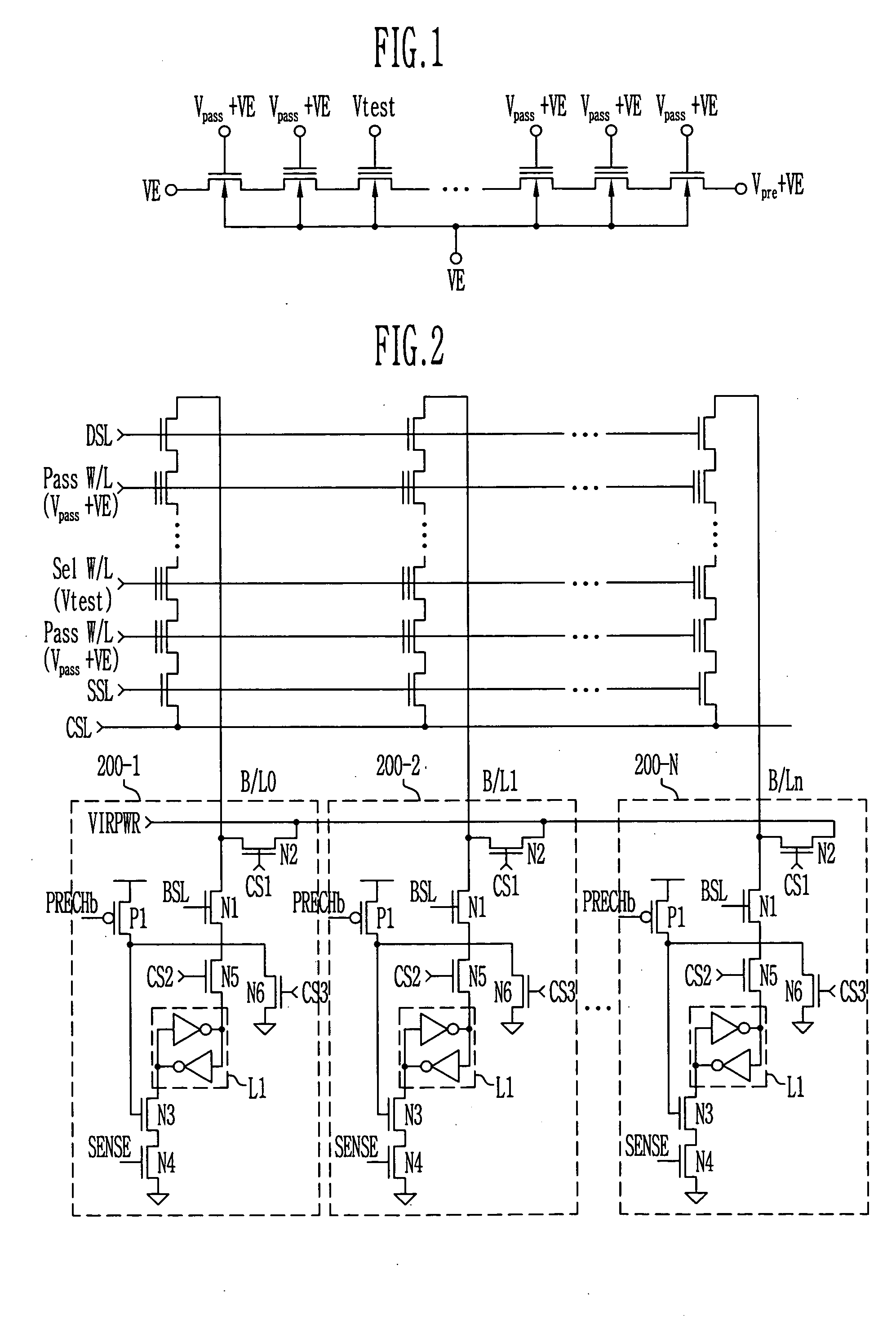
[0017]FIG. 1 is a schematic diagram illustrating a method for measuring a threshold voltage in a NAND flash memory device in accordance with the present invention.

[0018] Referring to FIG. 1, the NAND flash memory device includes a plurality of cell strings each of which is composed of a plurality of memory cells connected in series therein, a common drain node of the cell string, a common source node of the cell string, wordlines selecting the memory cells each by each,...


PUM


Abstract

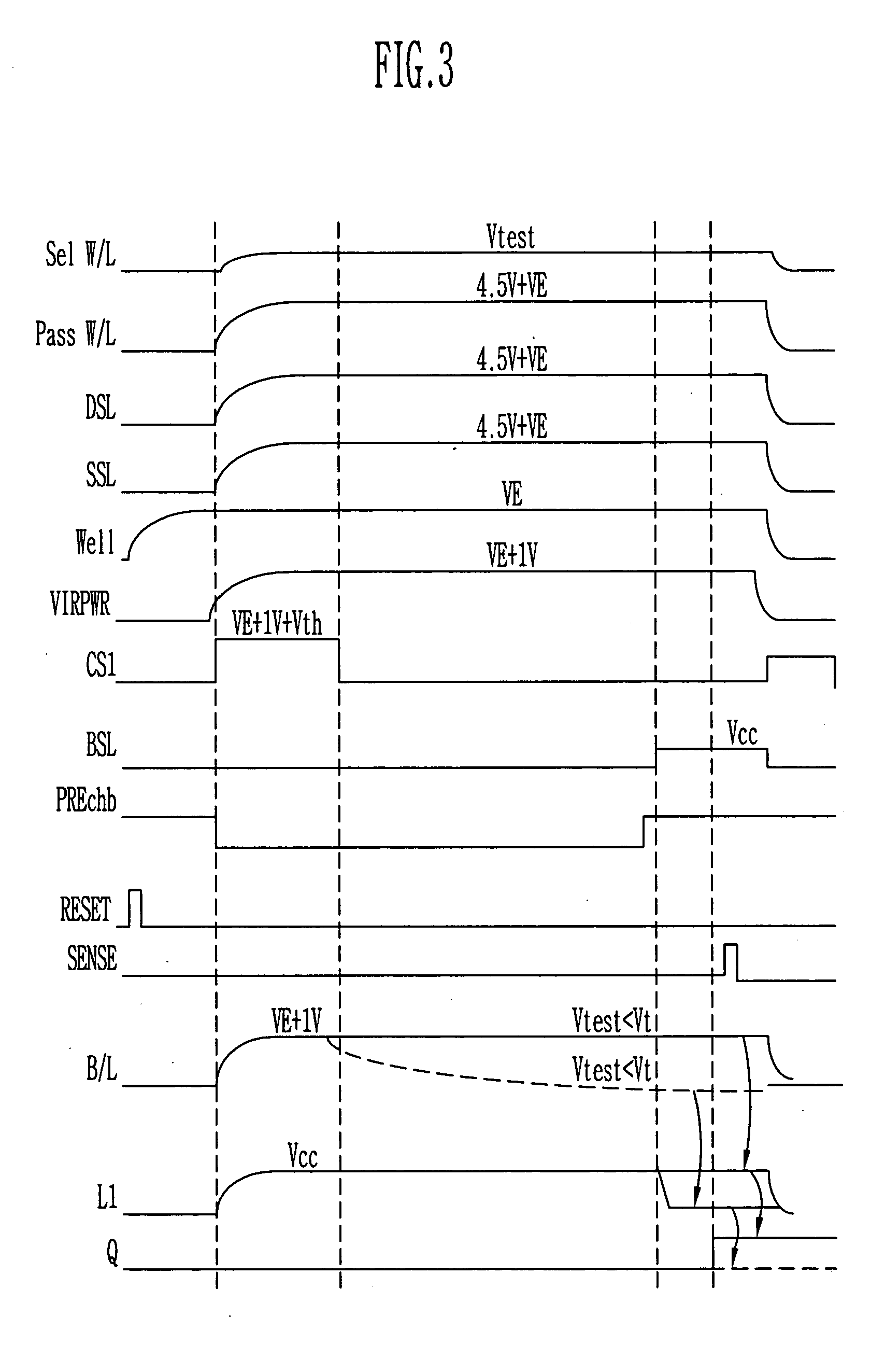
Provided is a method of measuring threshold voltages in a NAND flash memory device. In the method, a test voltage is applied to a wordline of selected memory cells to measure a distribution profile of threshold voltages of memory cells. A voltage summing up a pass voltage and an operation voltage is applied to wordlines of deselected cells. The operation voltage is applied to a well and a common source line. A voltage summing up a precharge voltage and the operation voltage is applied to a bitline. After then, a voltage variation on the bitline can be detected to measure a threshold voltage of a memory cell. A negative threshold voltage can be measured by applying a positive voltage with reference to a voltage, as the threshold voltage of the memory cell, set by subtracting the operation voltage from the test voltage in accordance with the bitline voltage variation.

Description

BACKGROUND [0001] 1. Field of the Invention [0002] The present invention relates to a method of measuring threshold voltages of a NAND flash memory device, and specifically, to a method of measuring a negative threshold voltage of an erased memory cell. [0003] 2. Discussion of Related Art [0004] In a NAND flash memory cell, threshold voltages of programmed memory cells distribute in the range of positive voltages higher than 0V, while threshold voltages of erased memory cells distribute in the range of negative voltages lower than 0V. For a NAND flash memory device, it is very important to measure distribution profiles of such threshold voltages in evaluating the reliability of memory cells. [0005] The NAND flash memory device needs wordline drivers constructed of NMOS transistors only in order to applying high voltages over 16V for programming the memory cells. However, the wordline drivers are incapable of transferring negative voltages to the wordlines. Therefore, as it is just a...

Claims


Application Information

Patent Timeline
Patent Type & Authority Applications(United States)
IPC IPC(8): G01R31/28G11C7/00G11C16/02G11C16/04G11C29/00G11C29/12G11C29/50
CPCG11C16/04G11C29/50004G11C29/50
Inventor PARK, JIN SUKIM, DOE COOK
Owner STMICROELECTRONICS SRL
Learn More