Multi-channel driver interface circuit for increasing phase count in a multi-phase DC-DC converter
- Summary
- Abstract
- Description
- Claims
- Application Information
AI Technical Summary
Benefits of technology
Problems solved by technology
Method used
Image
Examples
first embodiment
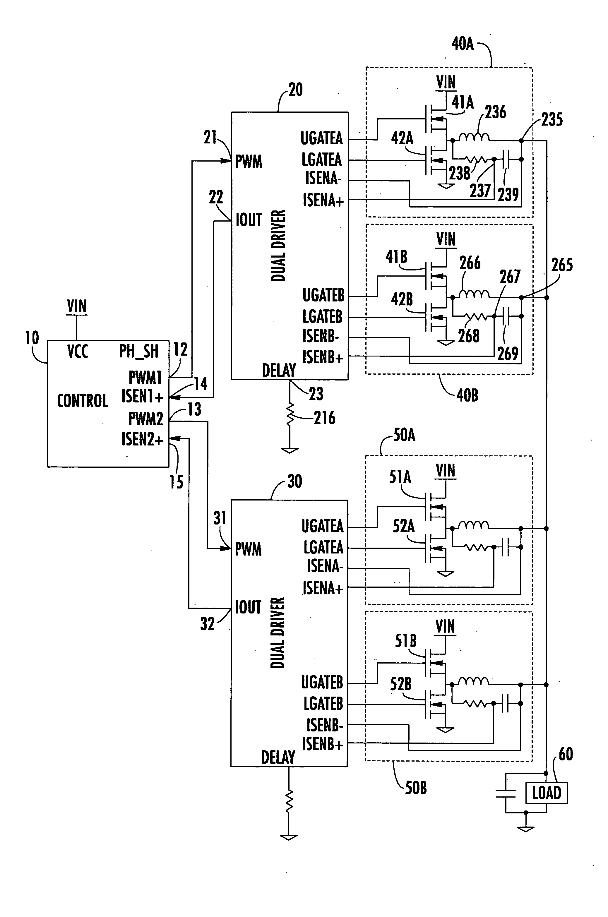
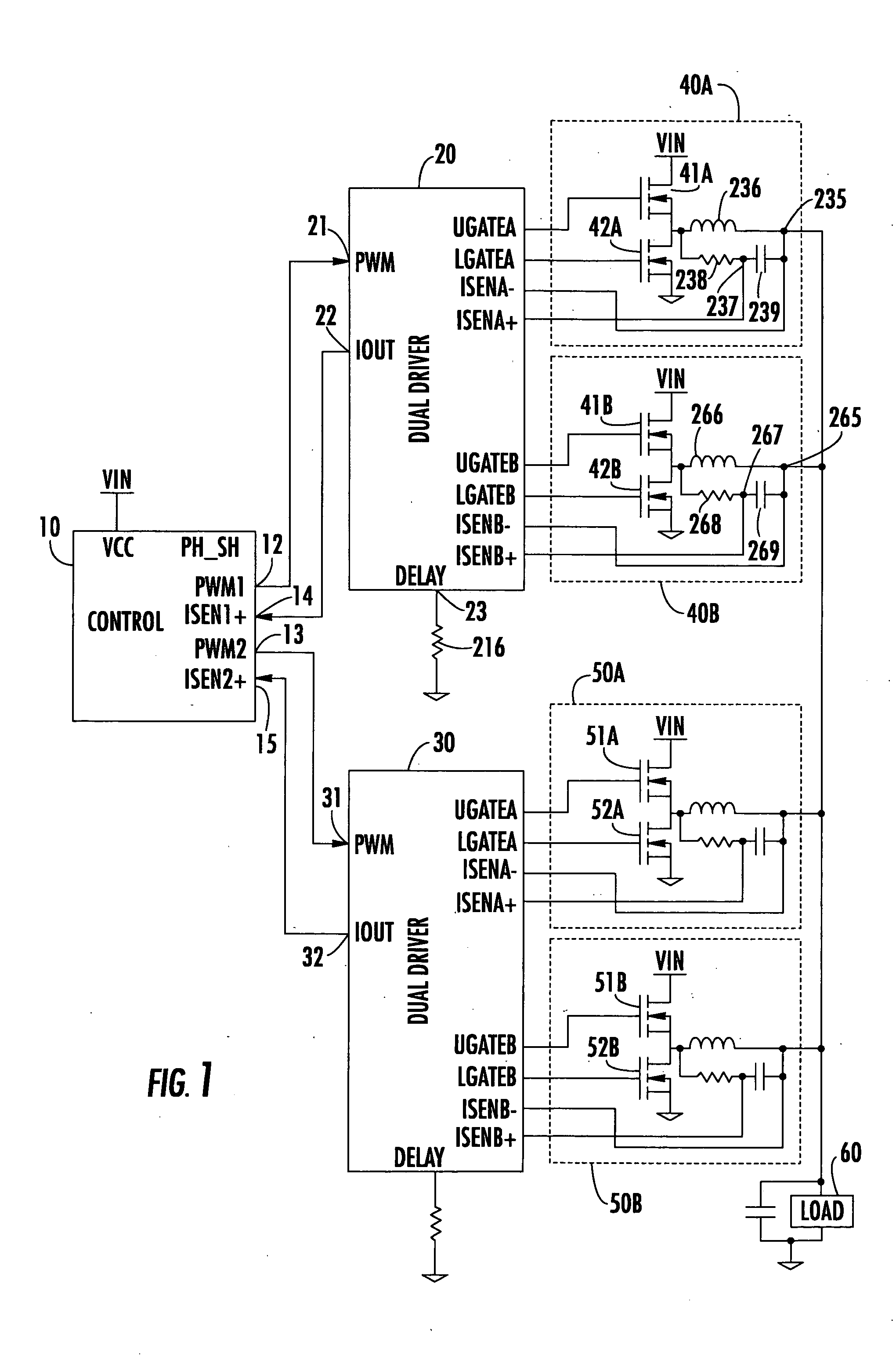
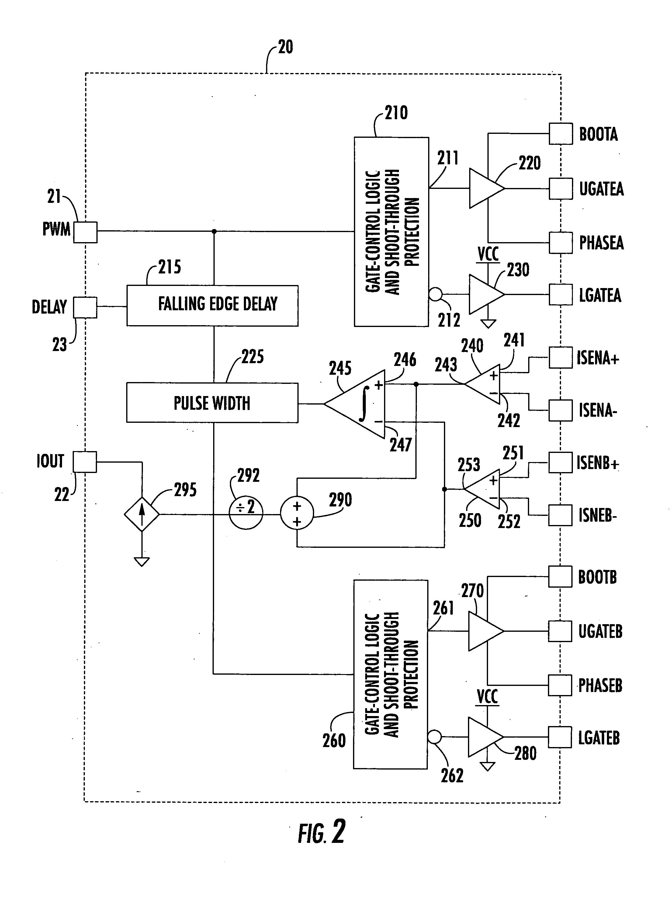
[0039] Attention is now further directed to FIG. 2, which shows the circuit architecture of each of the dual channel drivers 20 and 30. To reduce the complexity of the drawings, the following description will pertain to dual channel driver 20, it being understood that the description and illustration thereof applies equally to the dual channel driver 30 without any loss in generality. As shown in FIG. 2, the PWM input port 21, to which the PWM control signal is supplied from the supervisory controller 10, is coupled to a first A channel gate control logic section 210, which is of conventional configuration, and is used to apply gate or switching control signals to the ‘upper’ output channel switch 40A of the first pair of A and B channel switching circuits 40A and 40B.
[0040] For this purpose, gate control logic section 210 supplies a first output 211 through a first driver amplifier 220 to the UGATEA output for application to the gate of an upper MOSFET switch 41A of the A channel s...
second embodiment
[0053] As described above, in the circuit architecture of a respective dual channel driver shown in FIG. 2, the output of the error amplifier 245 is used to adjust the width of the channel B PWM signal, as output by delay circuit 215, prior to its being applied to the channel B gate control logic section 260. The output of the channel B gate control logic section is then used to control the gate drive signals for a respective one of switching circuit channels 40B and 50B. In accordance with a respective dual channel driver diagrammatically illustrated in FIG. 6, the output of the error amplifier 245 is used to control gate turn-off propagation delay of high side gate drive (for trailing edge PWM signals) or turn-off-delay of low side gate drive (for leading edge PWM signals), so as to provide current balance between the A and B channels. In the embodiment of FIG. 6, the pulse width control circuit 225 of FIG. 2 is replaced by combinational logic 300, which is effective to implement ...
PUM
 Abstract
Description
Claims
Application Information
 - R&D Engineer
- R&D Manager
- IP Professional
- Industry Leading Data Capabilities
- Powerful AI technology
- Patent DNA Extraction
Browse by: Latest US Patents, China's latest patents, Technical Efficacy Thesaurus, Application Domain, Technology Topic, Popular Technical Reports.
© 2024 PatSnap. All rights reserved.Legal|Privacy policy|Modern Slavery Act Transparency Statement|Sitemap|About US| Contact US: help@patsnap.com


