
Fitting substrate for connection and fitting substrate for connection for use in disk array control apparatus

Inactive Publication Date: 2005-04-21
HITACHI LTD
View PDF20 Cites 3 Cited by
  • Summary
  • Abstract
  • Description
  • Claims
  • Application Information

AI Technical Summary

Benefits of technology

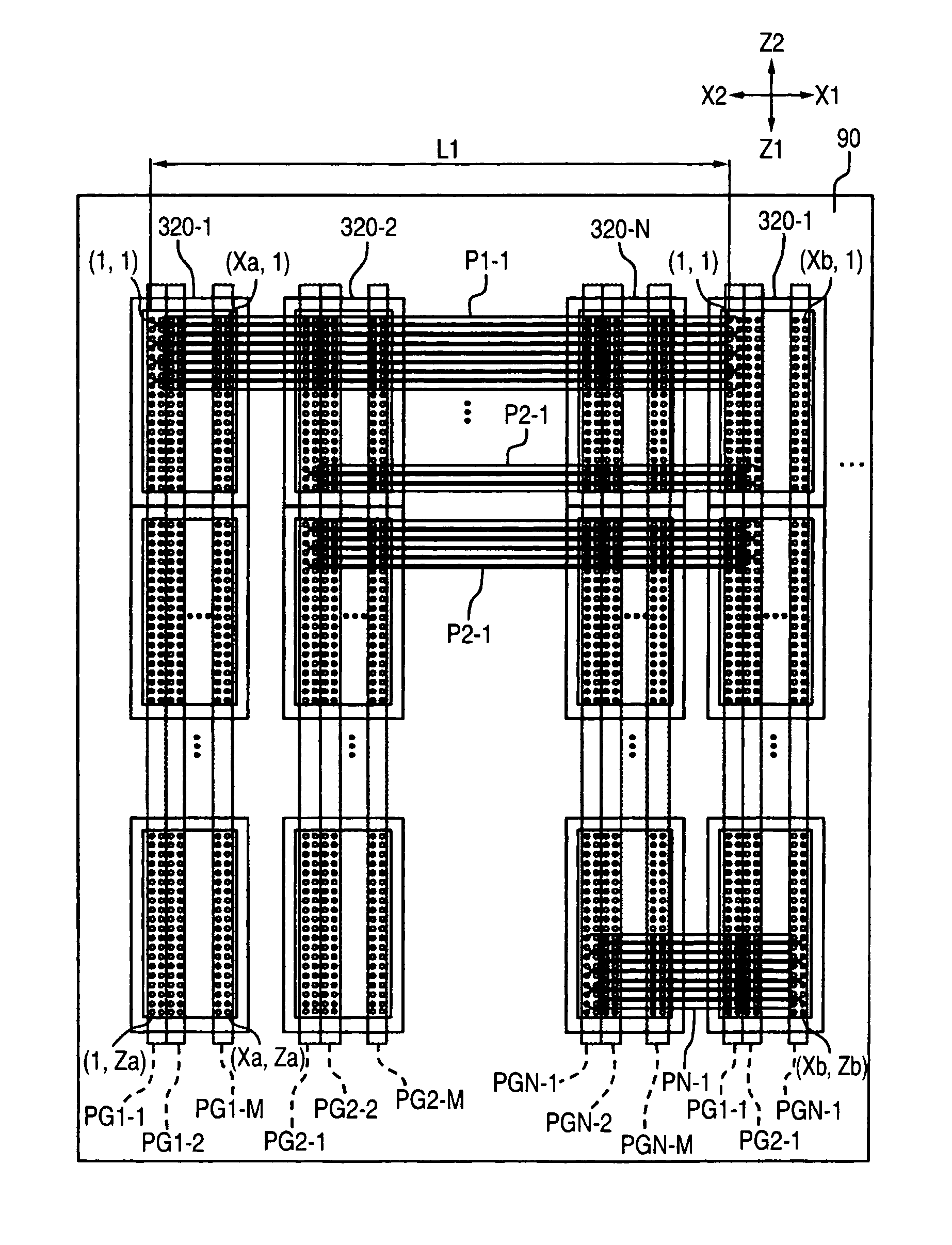
[0023] It is another object of the invention to provide a fitting substrate for connection and a fitting substrate for connection for use in a disk array control apparatus, the fitting substrate for connection capable of increasing the fitting number of signal processing substrates without inviting the increase of a size of the apparatus.

Problems solved by technology

Radiation noise is likely to occur at the curve point.
When the curve point exists in the printed wiring, signal quality is likely to drop.
However, because the wires for connecting the signal pins constituting the rows of the X coordinates=1 and the X coordinates=2 have already been arranged, wiring cannot be made on the same plane.
Consequently, a plurality of curve points occurs in each printed wiring and results in deterioration of signal quality.
Nonetheless, the market strongly needs a smaller disk array system having higher performance due to the limited size of the mounting space.

Method used


Image

  • Fitting substrate for connection and fitting substrate for connection for use in disk array control apparatus
  • Fitting substrate for connection and fitting substrate for connection for use in disk array control apparatus
  • Fitting substrate for connection and fitting substrate for connection for use in disk array control apparatus

Examples


first embodiment

1. First Embodiment

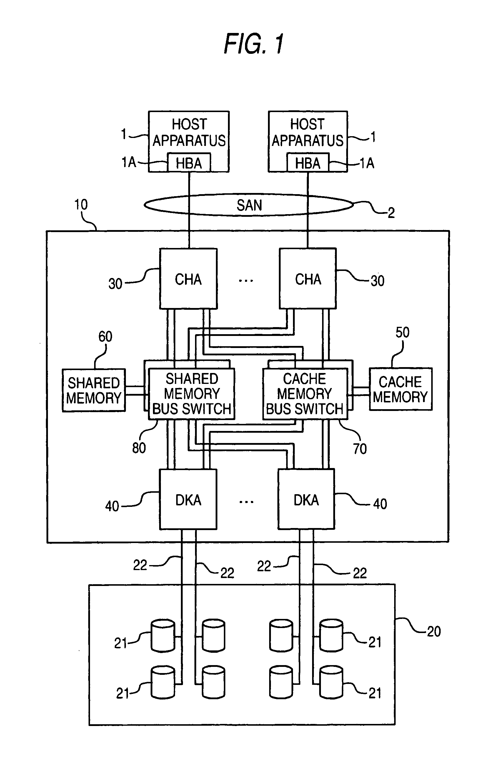
[0057] Referring to FIGS. 1 to 9, a first embodiment of the invention will be hereinafter explained about an example where the invention is applied to a disk control portion of a disk array subsystem. An overall construction of the disk array subsystem will be first explained, followed then by the explanation of a fitting state of various substrates.

[0058]FIG. 1 is a schematic block diagram showing a functional construction of the disk array subsystem. The disk array subsystem is broadly divided into a disk array control portion 10 and a disk apparatus 20. The disk array subsystem writes and reads data to and from the disk apparatus 20 in accordance with a request from a host apparatus 1 and transfers the data to the host apparatus 1.

[0059] Each host apparatus 1 is a CPU (Central Processing Unit) or a computer system equipped with memories, for example. Each host apparatus 1 uses a personal computer, a work station, a main frame or a mobile information terminal,...


PUM


Abstract

The invention efficiently mounts substrates to back planes and accomplishes high quality signal transfer. Connectors to which N adaptor substrates are fitted and connectors to which M bus switch substrates are fitted are provided to a multi-layered back plane. Signal pin groups of the connector on the adaptor substrate side are grouped into M data paths. Signal pins of the connector on the adaptor substrate side and corresponding signal pins of the connector on the bus switch substrate side are arranged horizontally in such a fashion as to exist on the same plane (with positions in a Z direction being substantially equal). Therefore, wiring patterns for connecting corresponding signal pins can be formed substantially linearly and a large number of substrates can be efficiently mounted to a limited area.

Description

CROSS-REFERENCES TO RELATED APPLICATIONS [0001] This application relates to and claims priority from Japanese Patent Application No. 2003-355902, filed on Oct. 16, 2003, the entire disclosure of which is incorporated herein by reference. BACKGROUND OF THE INVENTION [0002] 1. Field of the Invention [0003] This invention relates to a fitting substrate for connection to which a plurality of signal processing substrates is fitted. For instance, the invention relates to a fitting substrate for connection that will be suitable for use in a disk array control apparatus, or the like. [0004] 2. Description of the Related Art [0005] In an electronic appliance such as a disk control apparatus, for example, a plurality of signal processing substrates is fitted to accomplish respective functions. Known examples of such signal processing substrates include a memory substrate having cache memories and shared memories mounted thereto, a bus switch substrate for controlling access to the memory subs...

Claims


Application Information

Patent Timeline
IPC IPC(8): H05K1/02G06F1/18H05K1/14H05K7/06H05K7/14
CPCH05K7/1459
Inventor KOGA, TSUTOMUINOUE, MITSURUMINOWA, NOBUYUKI
Owner HITACHI LTD
Learn More