Liquid crystal display having wide viewing angle
a technology of liquid crystal display and viewing angle, which is applied in non-linear optics, instruments, optics, etc., can solve the problems of light leakage near the aperture, the contrast ratio of the conventional tn lcd in a normally black mode may not be so high,
- Summary
- Abstract
- Description
- Claims
- Application Information
AI Technical Summary
Benefits of technology
Problems solved by technology
Method used
Image
Examples
first embodiment
[0047] Now, the present invention will be described with reference to FIGS. 3-5.
[0048]FIG. 3 is a layout view of a common substrate of a liquid crystal display according to the first embodiment of the present invention. FIG. 3 shows a pixel region, where a common electrode has apertures.
[0049] As shown in FIG. 3, a black matrix pattern 7 is formed along the boundary of a pixel region P and a common electrode 6 is formed to cover the entire surface of the common substrate. The common electrode 6 has two longitudinally long linear apertures 15 which are spaced apart from and parallel to each other in a pixel region.
[0050] It is preferable that the width of the apertures 15 may be 3-15 μm, and the distance between the apertures 15 may be 8-50 μm. The width of 3-12 μm and the distance of 10-30 μm would be better.
[0051]FIG. 4 is a layout view of a TFT substrate according to the first embodiment of the present invention, and FIG. 5 is a sectional view of the TFT substrate taken along t...
second embodiment
[0055]FIGS. 6 and 7 are the respective layout views of the common and TFT substrates having horizontal apertures according to the
[0056] As shown in FIG. 6, a black matrix pattern 7 is formed along the boundary of a pixel region P, and a common electrode 6 is formed to cover the entire surface of the common substrate. The common electrode 6 has a plurality of horizontally long linear apertures 15 which are spaced apart from and parallel to each other in a pixel region.
[0057] The width and the distance of the apertures 15 may be the same as those of the first embodiment.
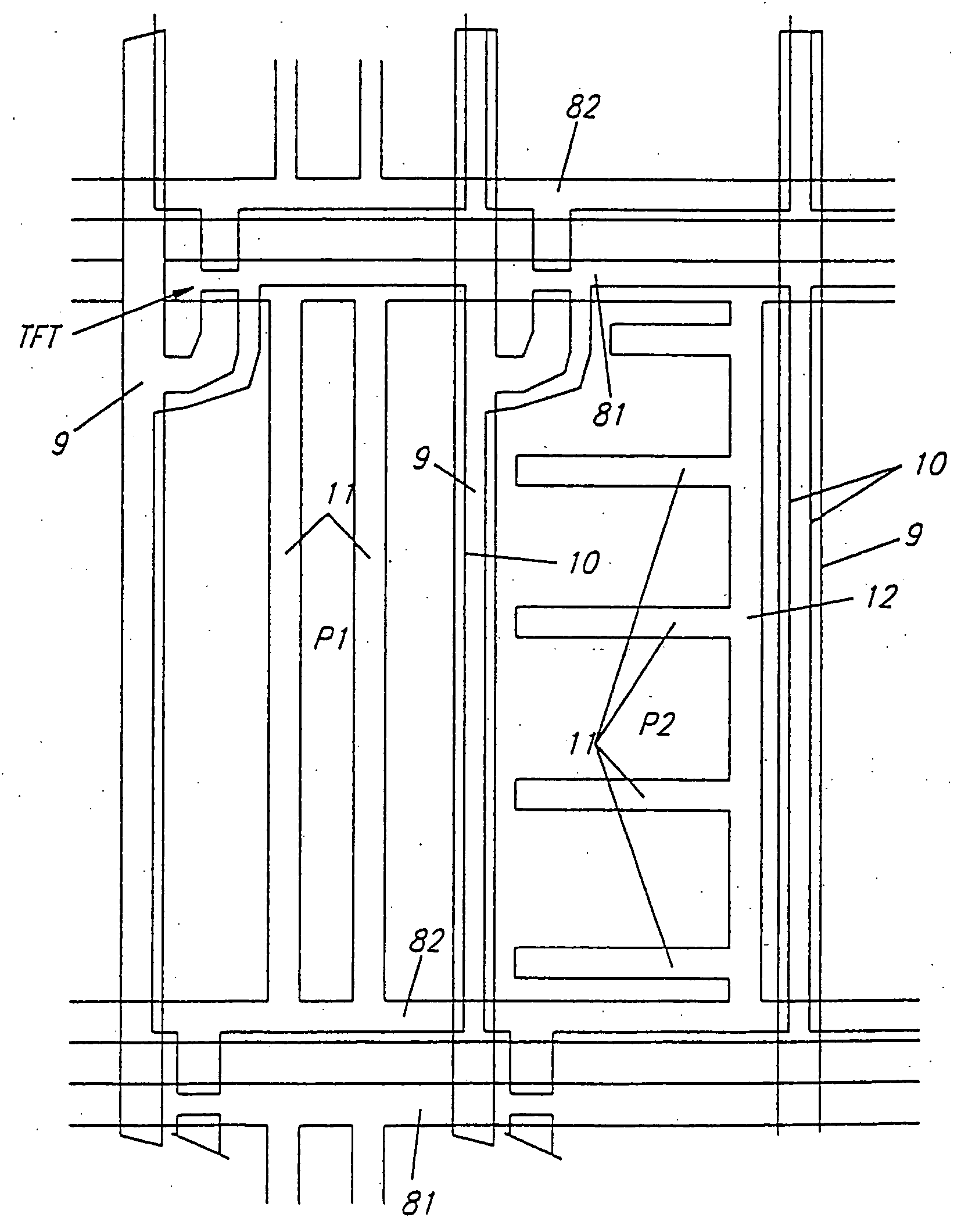
[0058] On the other hand, as shown in FIG. 7, a first and a second gate lines 81 and 82 which are separated from each other and extend horizontally and a branch 12 connecting the gate lines 81 and 82 extending in a vertical direction are formed on a transparent glass substrate 20. A plurality of storage capacitor electrodes 11 which are parallel to each other and to the gate lines 81 and 82 are formed on the substrat...
third embodiment
[0065] A TFT substrate illustrated in FIG. 11 has a first and a second gate lines 81 and 82, a branch 12 and a data line 9 having the same shapes as those in the third embodiment shown in FIG. 9. Two storage capacitor electrodes 11 parallel to each other extend obliquely in the up right or the bottom left direction and are connected to the branch 12.
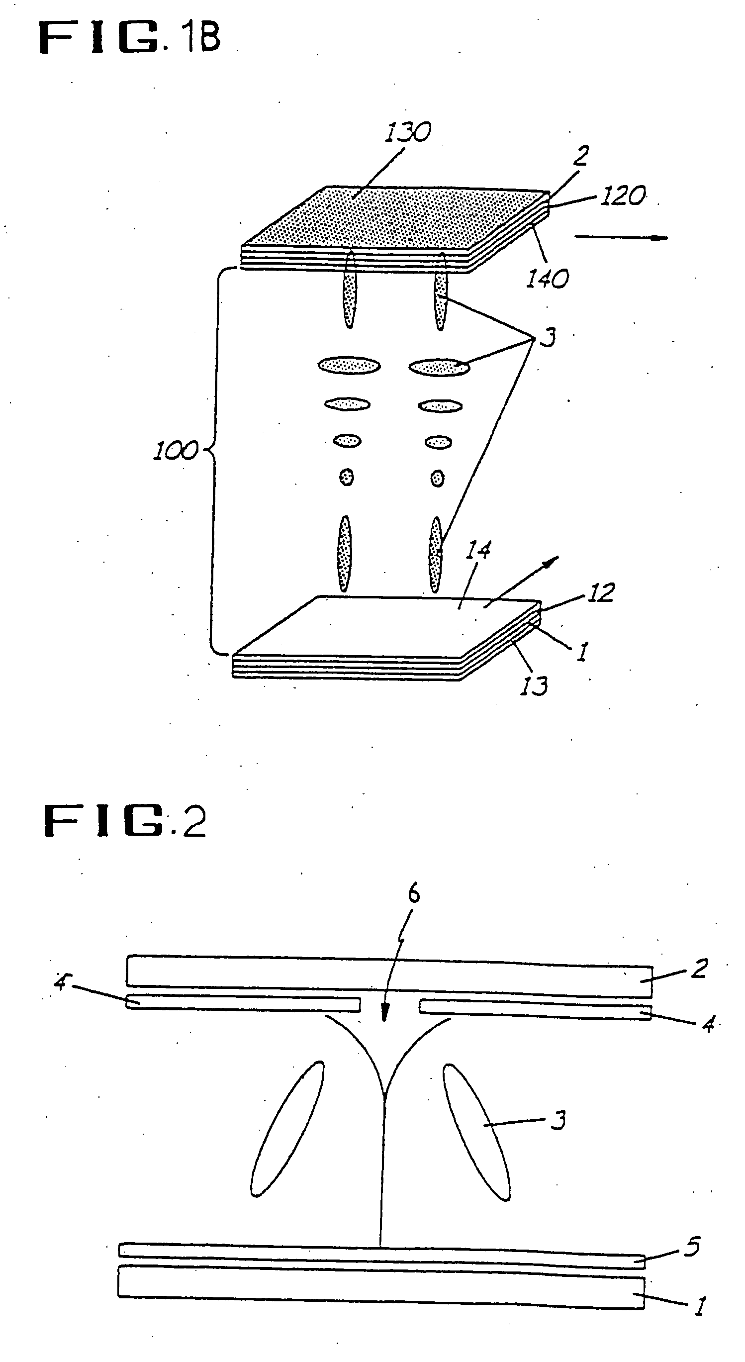
[0066] In the third and the fourth embodiments as in the first embodiment, the position of the storage capacitor electrodes 11 are corresponding to the apertures 15 in the common electrode 6 on the common substrate to shield the light leakage due to a fringe field.
[0067] In the third and the fourth embodiments of the present invention, the alignment layers formed on the pixel electrode may be rubbed or may not. When the alignment layers are rubbed, the rubbing direction may make an angle of 0°-135° with respect to the direction of the linear aperture.
[0068] Next, the fifth embodiment of the present invention will be described. In the f...
PUM
 Abstract
Description
Claims
Application Information
 - R&D
- Intellectual Property
- Life Sciences
- Materials
- Tech Scout
- Unparalleled Data Quality
- Higher Quality Content
- 60% Fewer Hallucinations
Browse by: Latest US Patents, China's latest patents, Technical Efficacy Thesaurus, Application Domain, Technology Topic, Popular Technical Reports.
© 2025 PatSnap. All rights reserved.Legal|Privacy policy|Modern Slavery Act Transparency Statement|Sitemap|About US| Contact US: help@patsnap.com


