
System and methed for effective field loss analysis for semiconductor wafers

a technology of loss analysis and semiconductor wafers, applied in the direction of testing/monitoring control systems, instruments, computing, etc., can solve the problems of insufficient total defect counts, microscopes or sems, and poor methodology for computing the effect of defects on yield, etc., to expedite the estimation of kill ratio and the effect of yield model

Inactive Publication Date: 2005-03-10
PROMOS TECH INC
View PDF5 Cites 8 Cited by
  • Summary
  • Abstract
  • Description
  • Claims
  • Application Information

AI Technical Summary

Benefits of technology

It is an object of the present invention to provide a method to predict yield loss with respect to yield impact upon selected defect density function according to defect classification on certain layer of a semiconductor wafer having a plurality of dies.

Problems solved by technology

However, the methodology for computing the effect of defects on yield was not well developed.
Defect counts are usually used to track excursions and set priorities for defect reduction efforts, but the total defect counts information on its own or even including further characterizations for each single defect by optical microscopes or SEM is not sufficient to control excursion.
Moreover, it is neither sufficient to assign an accurate number of yield loss according to the existing yield prediction models to each process for complex chip designs.
The review of all inspected defects may as well delay the manufacturing process of semiconductor chips and yield learning cycles significantly.
Unfortunately, practitioners in the semiconductor industry still hazily utilize the kill ratio concept.

Method used


Image

  • System and methed for effective field loss analysis for semiconductor wafers
  • System and methed for effective field loss analysis for semiconductor wafers
  • System and methed for effective field loss analysis for semiconductor wafers

Examples


Embodiment Construction

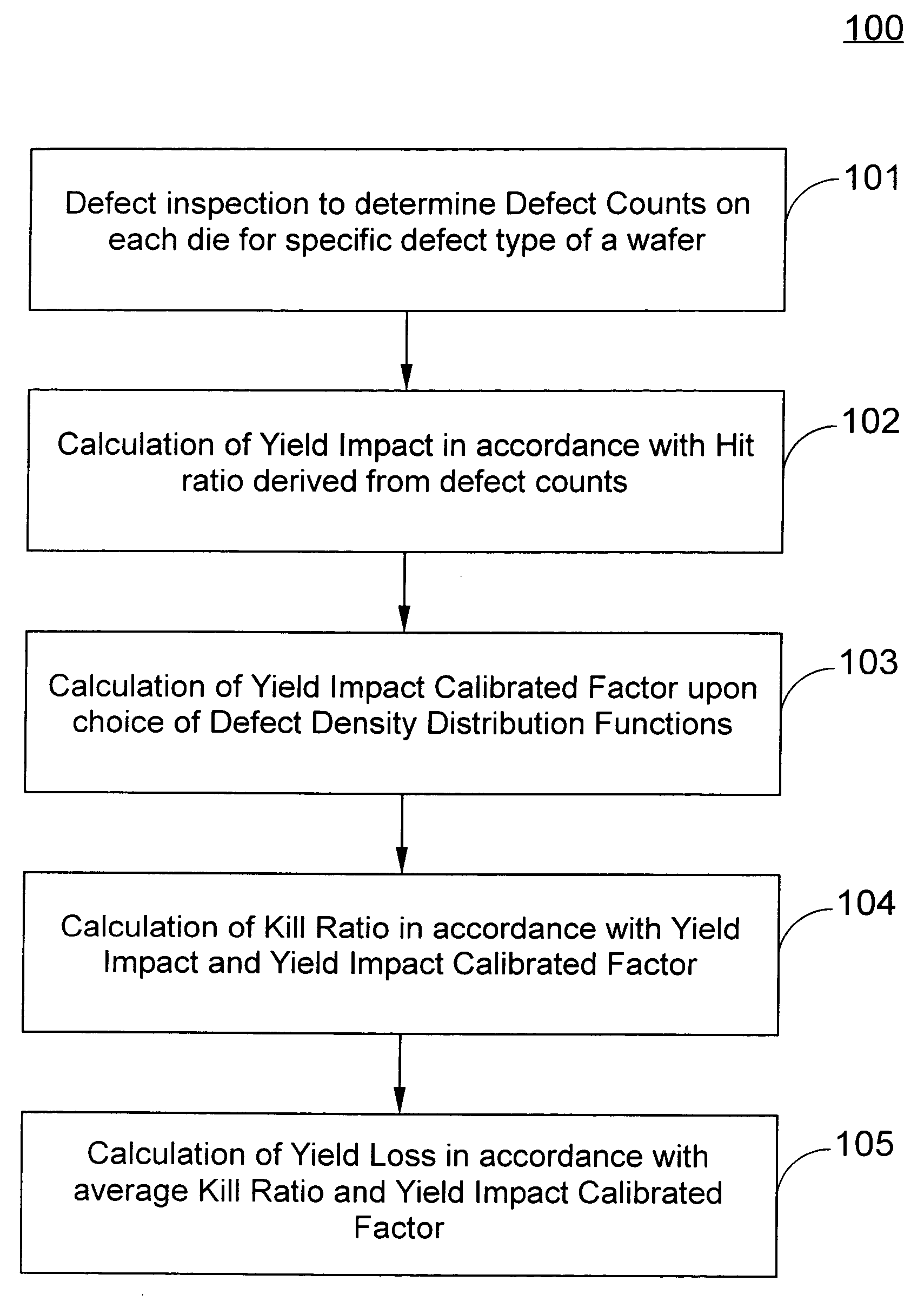
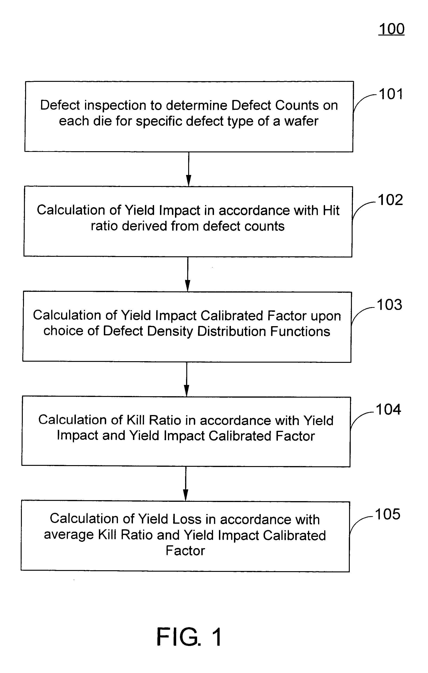
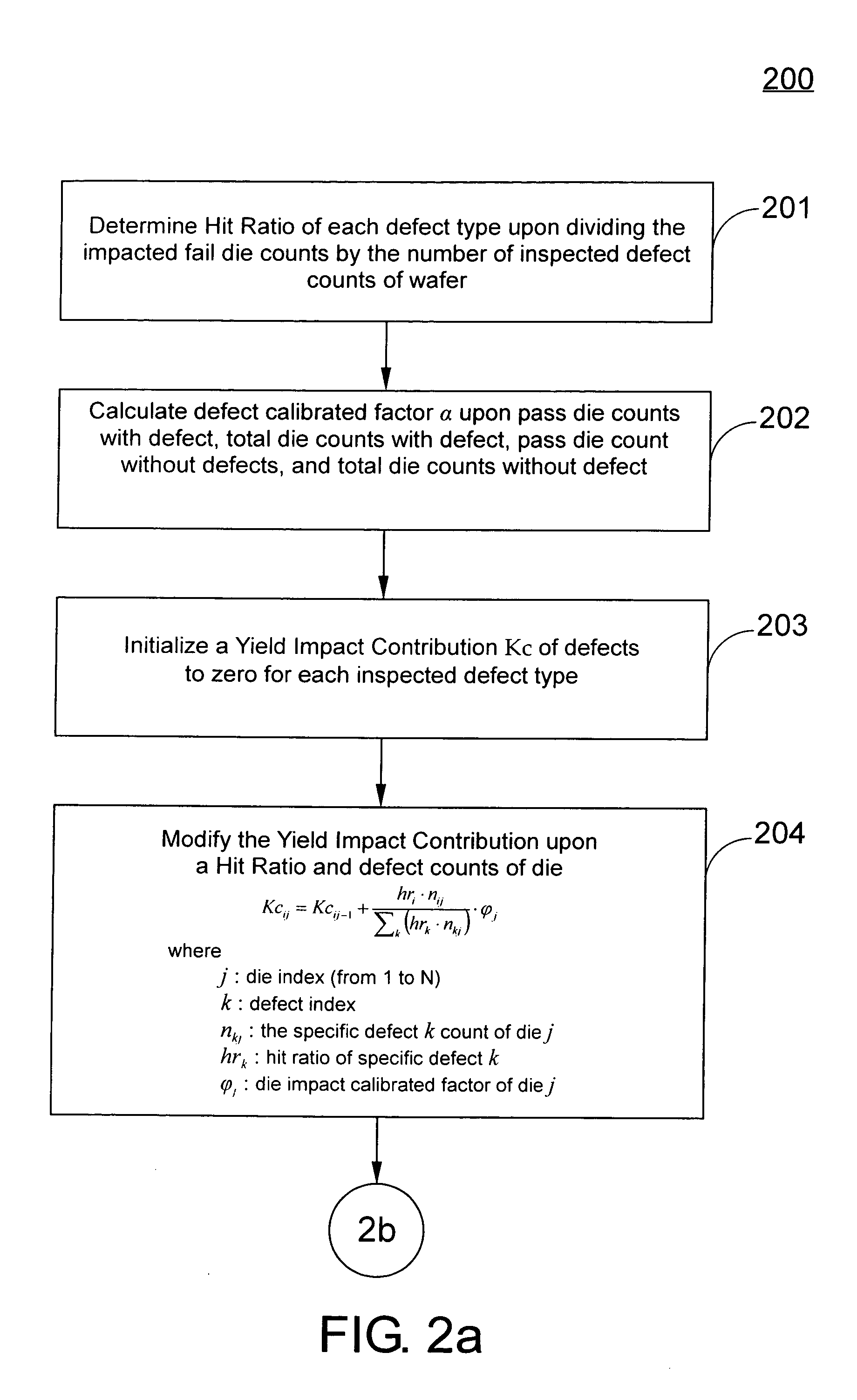
This disclosure relates to a yield loss analysis method of semiconductor wafers having a plurality of dies, and more particularly to a method for estimation of yield impact contributed by specific defect in order to predict yield loss. The present invention provides a method for “kill ratio” calculation according to defect counts for each defect type and die of a wafer. The present invention also provides a method for effective “kill ratio” calculation with the participation of defect contribution calibrated factor upon “die-based-sampling” technique. Lastly, the present invention provides a method determining yield loss upon selected defect density distribution model. The yield loss analysis method is described as follows.

Referring now in specific detail to the drawings in which like reference numerals identify similar or identical elements throughout the several views. Initially referring to FIG. 1, a flow / block diagram 100 is shown. In block 101, defects are reviewed by automa...


PUM


Abstract

This invention relates to a method for yield loss analysis of process steps of semiconductor wafers having a plurality of dies, and more particularly relates to a defect inspection technique to determine a hit ratio, computation of yield impact contributions for the defects, and determination of a kill ratio for a specific type of defect. Yield loss is estimated ultimately upon a choice of a defect density distribution function. A defect calibrated factor and a yield impact calibrated factor are introduced herein.

Description

BACKGROUND OF THE INVENTION 1. Field of Invention This present invention relates to a defect inspection and classification of semiconductor wafers having a plurality of dies. And more particularly, the present invention relates to a method for calculating yield impact contributed by specific defect type in order to predict yield loss effectively. 2. Description of Related Art Defect monitor methodology typically involves defect inspection and classification of defect types through optical microscope and Scanning Electron Microscope (SEM) review in order to control particles and defects that are inexpectant in production. In order to shorten the respond time and implement appropriate improvements for integrated circuits manufacturers, it is fairly important to establish an estimation scheme of various types of defects on the yield issue. This estimation scheme also allows an engineer to prioritize the defect reduction plan in the fabrication process. The first literature for yiel...

Claims


Application Information

Patent Timeline
Patent Type & Authority Applications(United States)
IPC IPC(8): G05B23/02G06F19/00
CPCG05B23/0221
Inventor WANG, WUN
Owner PROMOS TECH INC
Learn More