System and method for measuring the response time of a differential signal pair squelch detection circuit
a detection circuit and differential signal technology, applied in the field of system and method for measuring the response time of differential signal pair squelch detection circuit, can solve the problems of insufficient availability of specialized test equipment capable of measuring the response time, and the effect of reducing the overall testing time of a particular squelch detection circuit is minimal, and simple and accurate determination of the response tim
- Summary
- Abstract
- Description
- Claims
- Application Information
AI Technical Summary
Benefits of technology
Problems solved by technology
Method used
Image

Examples
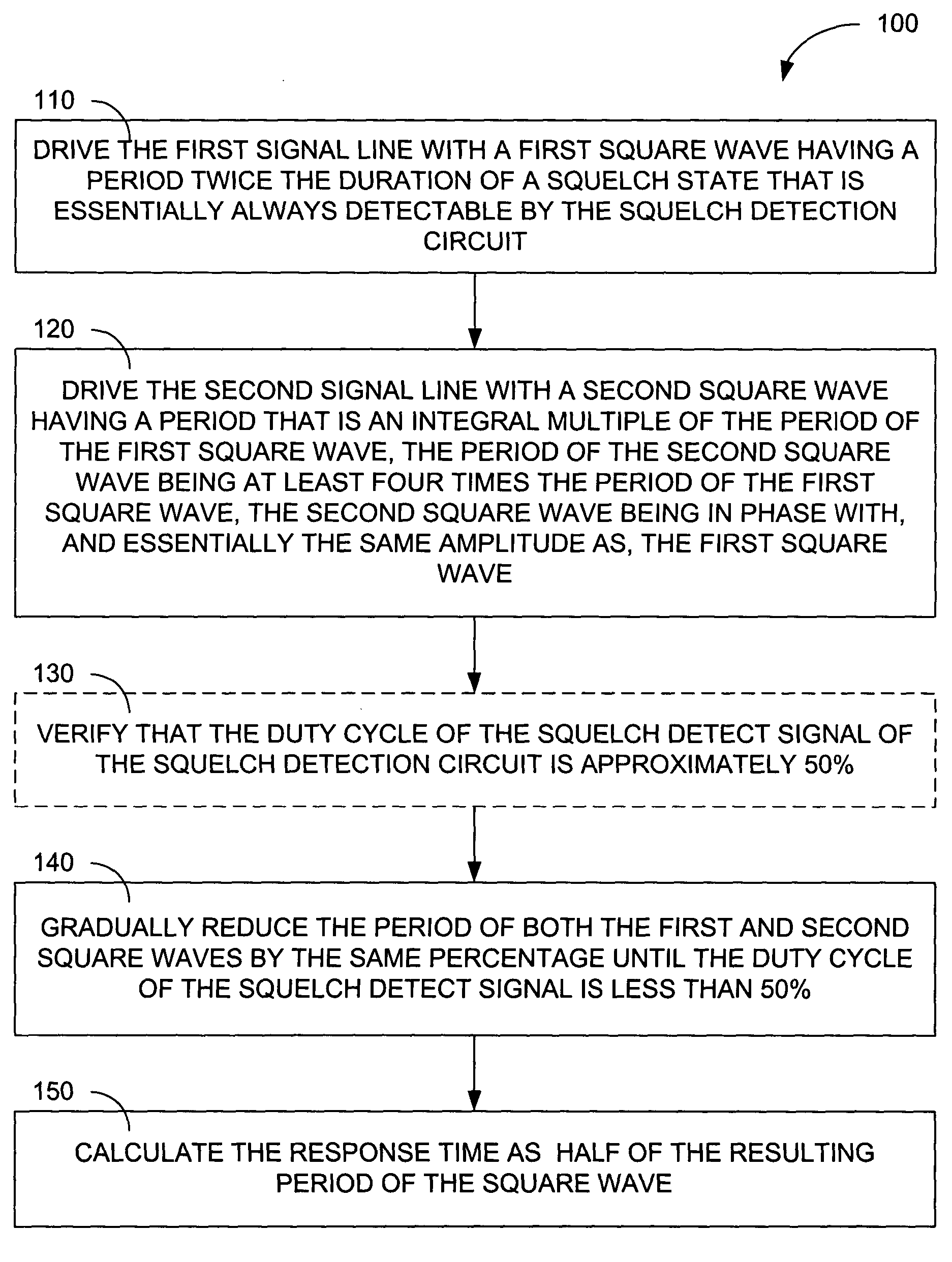
embodiment 100
[0025] In a first method embodiment 100 of FIG. 3, a first signal line, which may be either the positive or negative signal line, is driven with a first square wave having a period T that is twice the duration of a squelch state that is practically always detectable by the squelch detection circuit under test (step 110). A second square wave having a period that is an integral multiple of the period of the first square wave of at least 4T, in phase with and of the same amplitude as the first square wave, drives the remaining signal line (step 120).
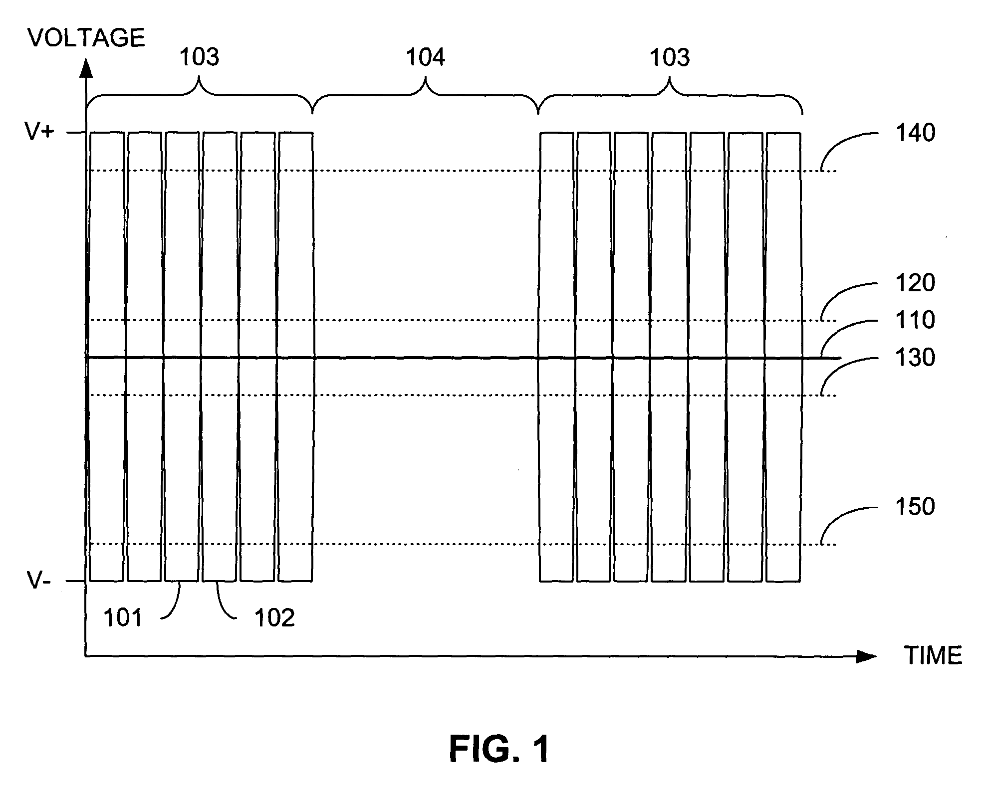
[0026] A specific example of the initial driving conditions of the method 100 is shown in FIG. 4. In this case, the positive (“p”) signal line is driven by the first square wave mentioned above. The second square wave of period 4T, which is in phase with the first square wave, drives the negative (“n”) signal line. The first and second square waves also have essentially the same amplitude so that a squelch state will be detected during tim...
embodiment 200
[0033]FIG. 8 shows an idealized set of waveforms of the first and second square waves resulting from the method embodiment 200 just as the duty cycle of the squelch detect signal begins to drop below the 50% level. At that point, the length of the shortest squelch states presented over the signal lines is half of the period of the first square wave in degrees, minus the final phase lag of the second square wave. This angular value is then divided by a full 360 degrees and multiplied by a full period of the first square wave to convert to a time value, thus representing the minimum response time of the squelch detection circuit under test.
[0034] The disclosed embodiments of the invention are appropriate primarily for testing squelch detection circuits that are insensitive to the direct-current (DC) value of the common mode voltage. The methods described produce the squelch state by driving both lines of the differential signal pair to either V+ or V−, as opposed to the midpoint volta...
PUM
 Abstract
Description
Claims
Application Information
 - R&D
- Intellectual Property
- Life Sciences
- Materials
- Tech Scout
- Unparalleled Data Quality
- Higher Quality Content
- 60% Fewer Hallucinations
Browse by: Latest US Patents, China's latest patents, Technical Efficacy Thesaurus, Application Domain, Technology Topic, Popular Technical Reports.
© 2025 PatSnap. All rights reserved.Legal|Privacy policy|Modern Slavery Act Transparency Statement|Sitemap|About US| Contact US: help@patsnap.com