Liquid crystal display device

Inactive Publication Date: 2005-03-03
SHARP KK
View PDF14 Cites 20 Cited by
  • Summary
  • Abstract
  • Description
  • Claims
  • Application Information

AI Technical Summary

Benefits of technology

[0021] The present invention was made to solve the above conventional problems, and an object of the invention is to provide a liquid crystal display device in which alignment control is efficiently carried out between picture element electrodes. The present invention therefore provides a liquid crystal display device that can realize domain division with strong alignment regulating force and superior response characteristics, without forming a projection on the bus line and without lowering aperture ratio.
[0026] That is, in the present invention, the alignment of the liquid crystal molecules is controlled by effectively using the oblique electric fields generated by the aperture portions, in other words, the oblique electric fields generated by the edges of the picture element electrodes.
[0030] Therefore, there will be no alignment disturbance in the liquid crystal domains formed on the picture element electrodes which overlap with the bus lines. As a result, it is possible to suppress decrease of response speed (deterioration of response characteristics) and generation of the afterimage phenomenon.
[0032] Therefore, by effectively controlling alignment of the picture element electrodes, the liquid crystal display device can realize domain division without forming projections on the bus lines and without lowering aperture ratio. The domain division can also be realized with strong alignment regulating force for the liquid crystal and with superior response characteristics.

Problems solved by technology

However, in the conventional liquid crystal display device disclosed in Japanese Patent No. 2947350, there is the problem of increased manufacturing steps, because the projection 304 needs to be formed on the data bus line 303.
As a result, there is a problem that the alignment needs to be controlled by forming projections on the data bus line 303 of the counter electrode.
As a result, there is a problem that the aperture ratio decreases.

Method used


Image

  • Liquid crystal display device
  • Liquid crystal display device
  • Liquid crystal display device

Examples


Embodiment Construction

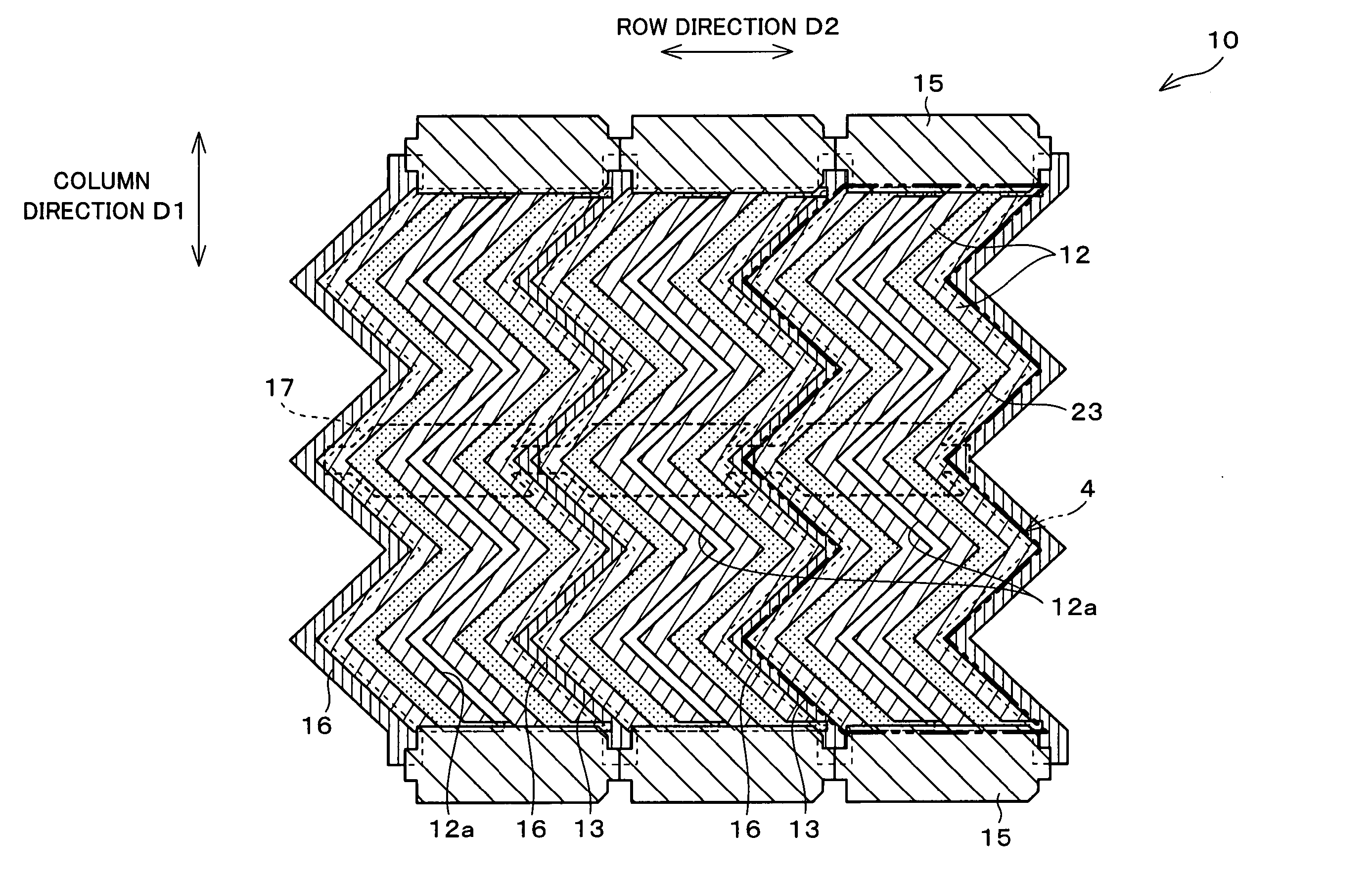
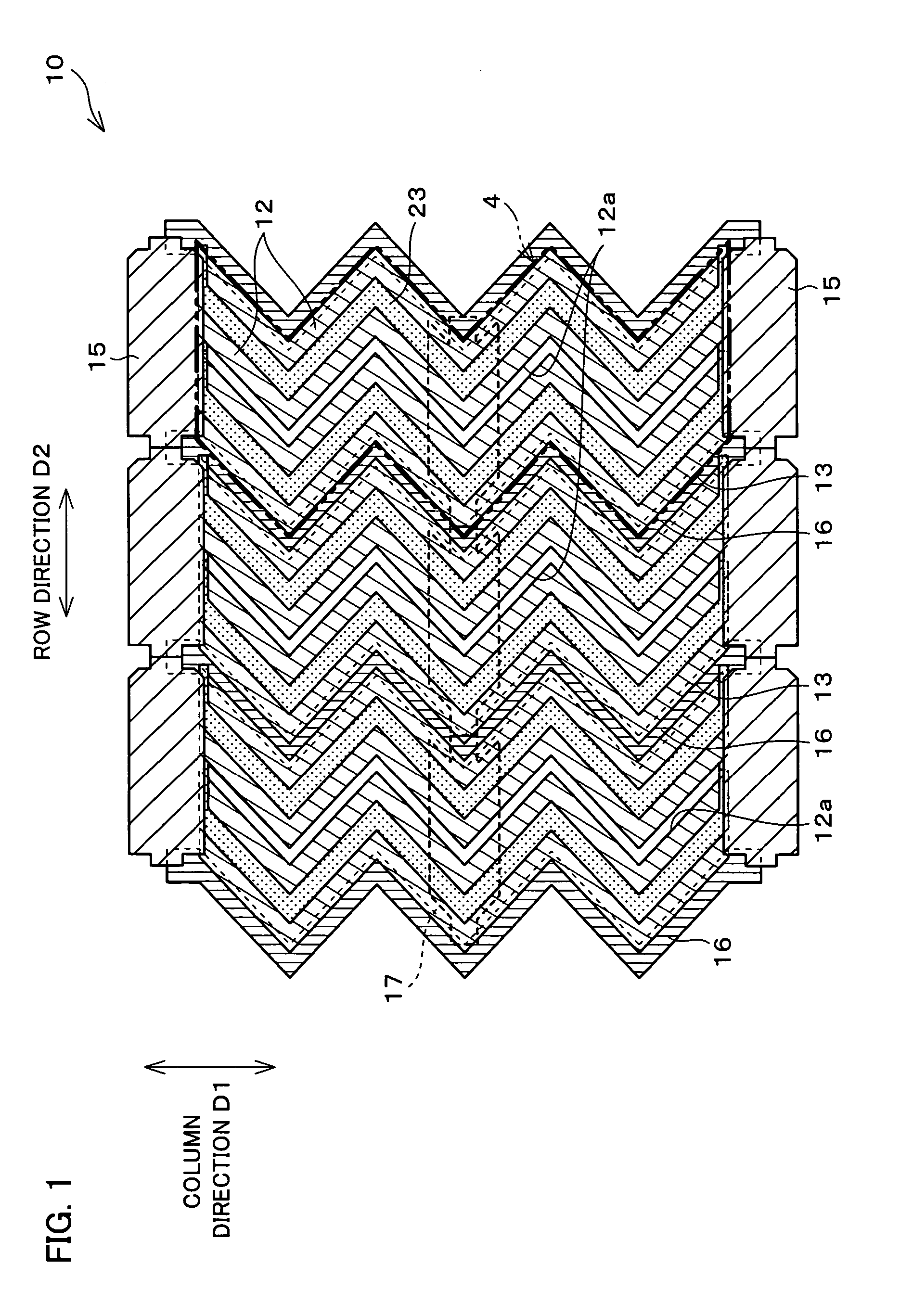
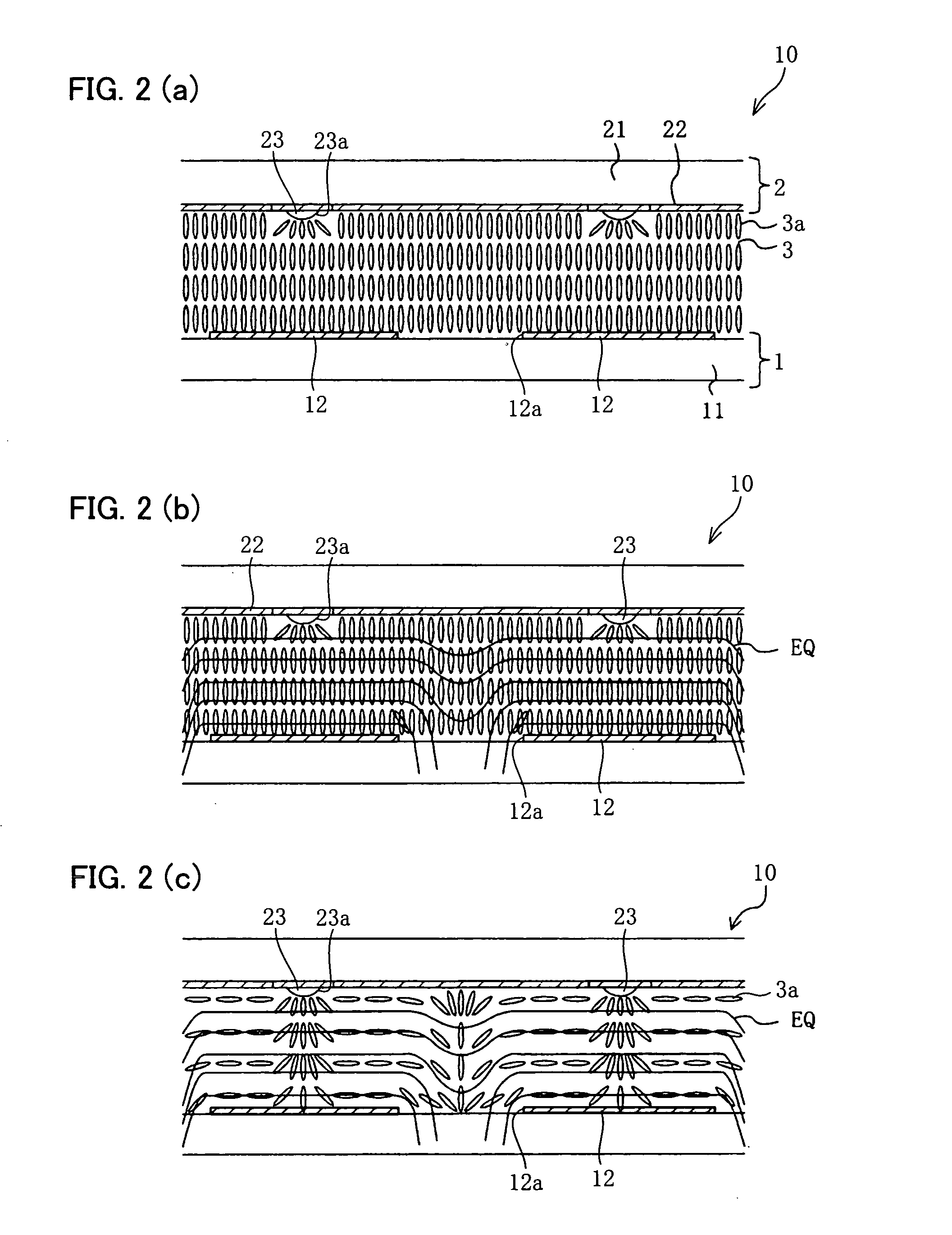
[0055] The following description deals with one embodiment of the present invention with reference to FIGS. 1 through 9. Note that, an active matrix type liquid crystal display device using a thin film transistor (TFT) is explained in the present embodiment. Moreover, a transmissive liquid crystal display device is explained as an example; however, the present invention is not limited to this and is also applicable to a reflective liquid crystal display device and a transflective liquid crystal display device. Furthermore, the present invention is applicable to a liquid crystal display device employing either a normally black mode or normally white mode.

[0056] Moreover, as used herein, the term “picture element region” is used to mean a region of the liquid crystal display device which corresponds to a “picture element,” which is a minimum unit of display. In a color liquid crystal display device, “picture elements” of R, G, and B correspond to a single “pixel.” In the active matri...


PUM


Abstract

In a liquid crystal display device of the present invention, when a display voltage is applied to picture element electrodes, each picture element electrode forms a plurality of domains in which liquid crystal molecules align themselves in different directions. The picture element electrodes are formed such that their edge portions on the opposite sides of a picture-element-electrode aperture portion formed between the picture element electrodes face parallel to each other with a certain interval. A source bus line is provided along the picture-element-electrode aperture portion formed between the picture element electrodes. The source bus line is disposed beneath the picture element electrodes and at the edge portions of the picture element electrodes by overlapping therewith in a direction of thickness.

Description

[0001] This Nonprovisional application claims priority under 35 U.S.C. § 119(a) on Patent Application No. 2003 / 209340 filed in Japan on Aug. 28, 2003, the entire contents of which are hereby incorporated by reference. FIELD OF THE INVENTION [0002] The present invention relates to a liquid crystal display device and, more particularly, to a liquid crystal display device of a so-called multi-domain vertical alignment mode. BACKGROUND OF THE INVENTION [0003] Conventionally available are liquid crystal display devices of a VA (Vertical Alignment) mode using a vertical alignment film, offering good contrast, good working speed, and good viewing angle characteristics. In recent years, in order to increase viewing angle, there has been developed a multi-domain technique, in which a display pixel is divided into a plurality of domains and the alignment of liquid crystal is varied in these domains. [0004] There are mainly two kinds of substrate structure which can realize such a multi-domain...

Claims


Application Information

Patent Timeline
IPC IPC(8): G02F1/139G02F1/133G02F1/1333G02F1/1337G02F1/1343G09F9/30G09F9/35
CPCG02F1/133707G02F2001/133776G02F1/134336G02F1/133776G02F1/1337
Inventor KUBO, MASUMIYAMAMOTO, AKIHIRO
Owner SHARP KK
Why Eureka
Try Eureka