Arrays of protein-capture agents and methods of use thereof
a protein and protein technology, applied in the field of arrays of protein capture agents, can solve the problems of large sample sizes, time-consuming, and limited in its ability to reproduce a significant fraction, and achieve the effect of improving reproducibility, improving reproducibility, and improving the quality of the sampl
- Summary
- Abstract
- Description
- Claims
- Application Information
AI Technical Summary
Problems solved by technology
Method used
Image
Examples
example 1
Fabrication of a Two-dimensional Array by Photolithography
[0214] In a preferred embodiment of the invention, two-dimensional arrays are fabricated onto the substrate material via standard photolithography and / or thin film deposition. Alternative techniques include microcontact printing. Usually, a computer-aided design pattern is transferred to a photomask using standard techniques, which is then used to transfer the pattern onto a silicon wafer coated with photoresist.
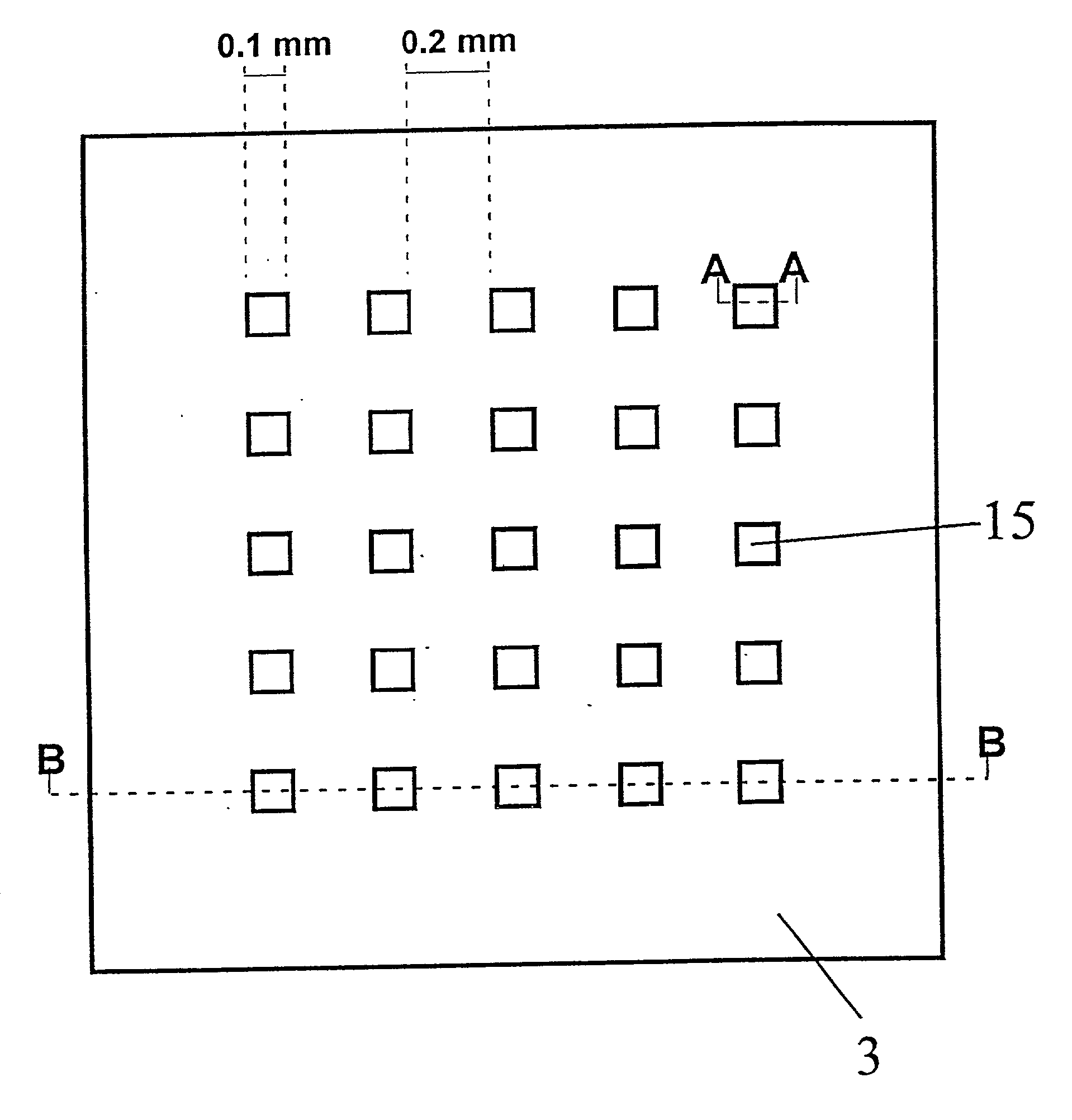
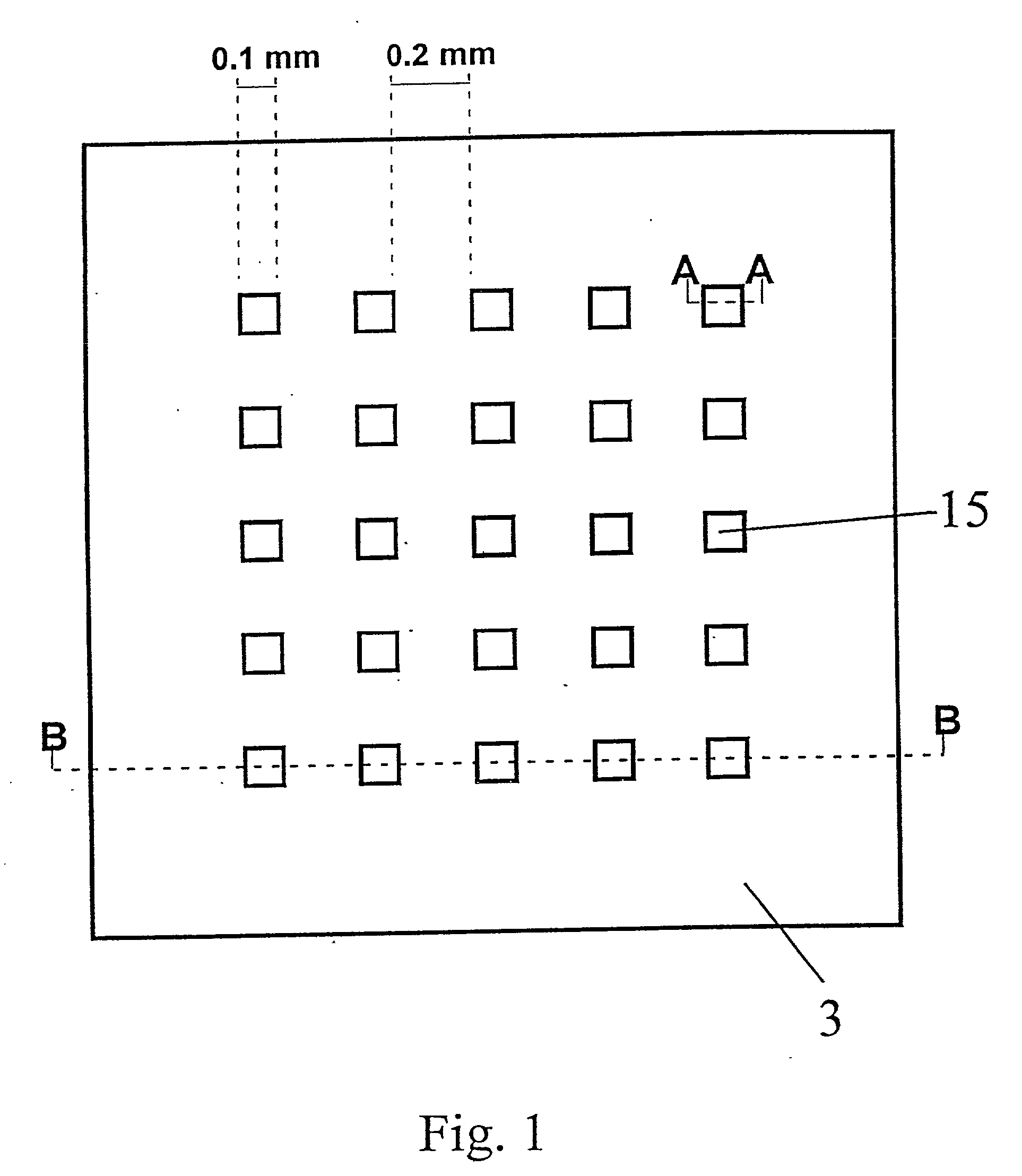
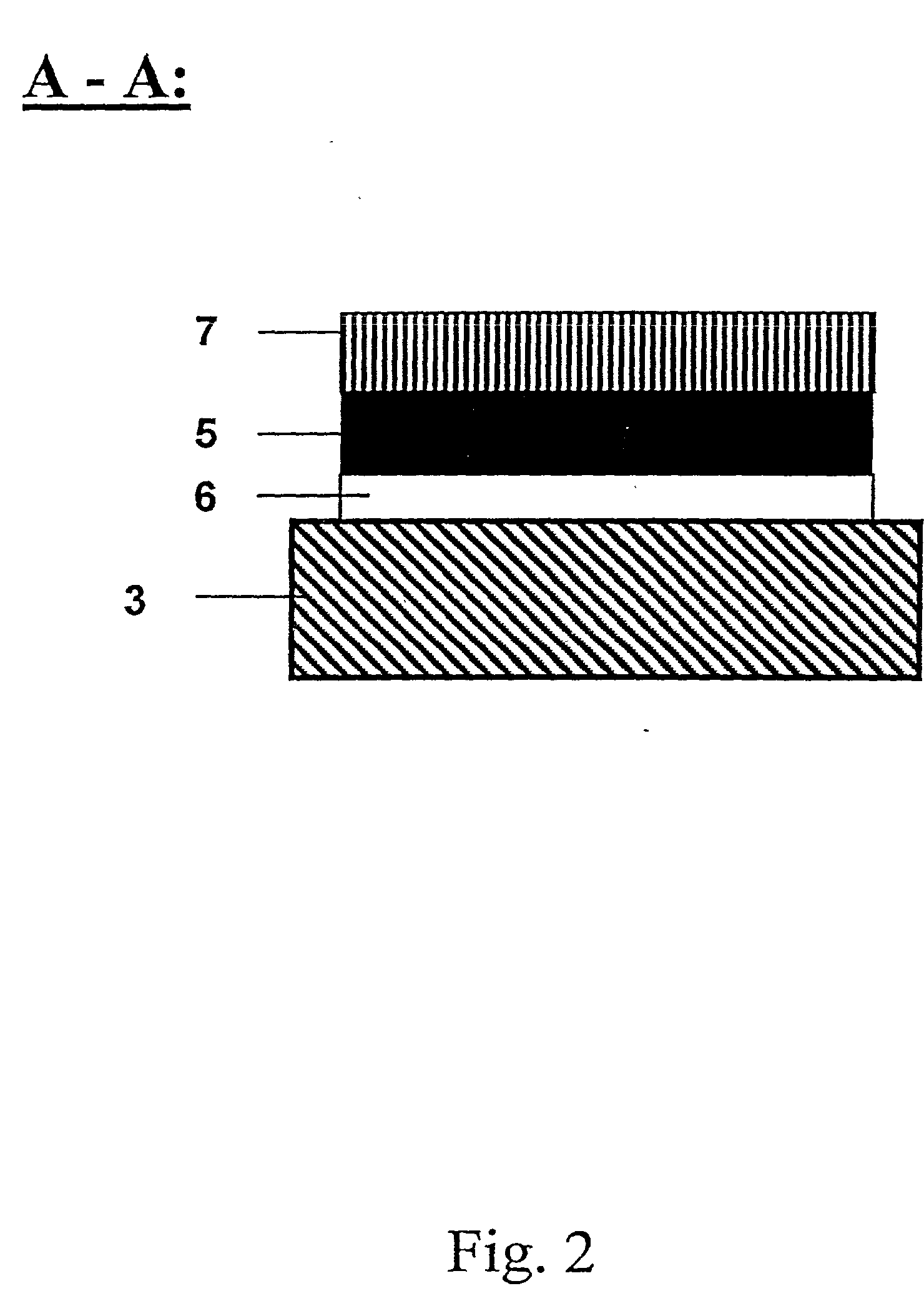
[0215] In a typical example, the array ("chip") with lateral dimensions of 10.times.10 mm comprises squared patches of a bioreactive layer (here: gold as the coating on a silicon substrate) each 0.1.times.0.1 mm in size and separated by hydrophobic surface areas with a 0.2 mm spacing. 4" diameter Si(100) wafers (Virginia Semiconductor) are used as bulk materials. Si(100) wafers are first cleaned in a 3:1 mixture of H.sub.2SO.sub.4, conc.: 30% H.sub.2O.sub.2 (90.degree. C., 10 min), rinsed with deionized water (18 M.OM...
example 2
Fabrication of a Two-dimensional Array by Deposition Through a Hole Mask
[0216] In another preferred embodiment the array of gold patches is fabricated by thin film deposition through a hole mask which is in direct contact with the substrate. In a typical example, Si(100) wafers are first cleaned in a 3:1 mixture of H.sub.2SO.sub.4, conc.: 30% H.sub.2O.sub.2 (90.degree. C., 10 min), rinsed with deionized water (18 M.OMEGA.cm), finally passivated in 1% aqueous HF and singed at 150.degree. C. for 30 min to become hydrophobic. The wafer is then brought into contact with a hole mask exhibiting the positive pattern of the desired patch array. In the next step, the wafer is primed with a titanium layer of 20 nm thickness, followed by a 200 nm thick gold layer. Both layers were deposited using electron-beam evaporation (5 .ANG. / s). After removal of the mask, the gold patches can be further chemically modified to achieve the desired bioreactive and biocompatible properties (see Example 3, be...
example 3
Synthesis of an Aminoreactive Monolayer Molecule (Following the Procedure Outlined in Wagner et al., Biophys. J., 1996, 70:2052-2066)
[0217] General. .sup.1H- and .sup.13C-NMR spectra are recorded on Bruker instruments (100 to 400 MHz). Chemical shifts (.delta.) are reported in ppm relative to internal standard ((CH.sub.3).sub.4Si, .delta.=0.00 (.sup.1H- and .sup.13C-NMR)). FAB-mass spectra are recorded on a VG-SABSEQ instrument (Cs.sup.+, 20 keV). Transmission infrared spectra are obtained as dispersions in KBr on an FTIR Perkin-Elmer 1600 Series instrument. Thin-layer chromatography (TLC) is performed on precoated silica gel 60 F254 plates (MERCK, Darmstadt, FRG), and detection was done using Cl.sub.2 / toluidine, PdCl.sub.2 and UV-detection under NH.sub.3-vapor. Medium pressure liquid chromatography (MPLC) is performed on a Labomatic MD-80 (LABOMATIC INSTR. AG, Allschwil, Switzerland) using a Buechi column (460.times.36 mm; BUECHI, Flawil, Switzerland), filled with silica gel 60 (pa...
PUM
| Property | Measurement | Unit |
|---|---|---|
| area | aaaaa | aaaaa |
| area | aaaaa | aaaaa |
| area | aaaaa | aaaaa |
Abstract
Description
Claims
Application Information
 - R&D
- Intellectual Property
- Life Sciences
- Materials
- Tech Scout
- Unparalleled Data Quality
- Higher Quality Content
- 60% Fewer Hallucinations
Browse by: Latest US Patents, China's latest patents, Technical Efficacy Thesaurus, Application Domain, Technology Topic, Popular Technical Reports.
© 2025 PatSnap. All rights reserved.Legal|Privacy policy|Modern Slavery Act Transparency Statement|Sitemap|About US| Contact US: help@patsnap.com


