
Workpiece distribution and processing in a high throughput stacked frame

a stacking frame and workpiece technology, applied in the field of semiconductor processing systems, can solve the problems of large floor space occupied by the system as a whole, high cost, scarce land, etc., and achieve the effect of increasing the cost of providing a sufficiently large clean room

Inactive Publication Date: 2002-09-26
APPLIED MATERIALS INC
View PDF11 Cites 30 Cited by
  • Summary
  • Abstract
  • Description
  • Claims
  • Application Information

AI Technical Summary

Problems solved by technology

However, because of the relatively large number of chambers and the irregular pentagonal shape, the system as a whole can occupy a substantial amount of floor space.
This can be a particular problem in locations where land is very scarce and / or very expensive.
In addition, because wafer processing is preferably performed in clean room conditions, providing a sufficiently large clean room can further substantially increase costs.

Method used


Image

  • Workpiece distribution and processing in a high throughput stacked frame
  • Workpiece distribution and processing in a high throughput stacked frame
  • Workpiece distribution and processing in a high throughput stacked frame

Examples


Embodiment Construction

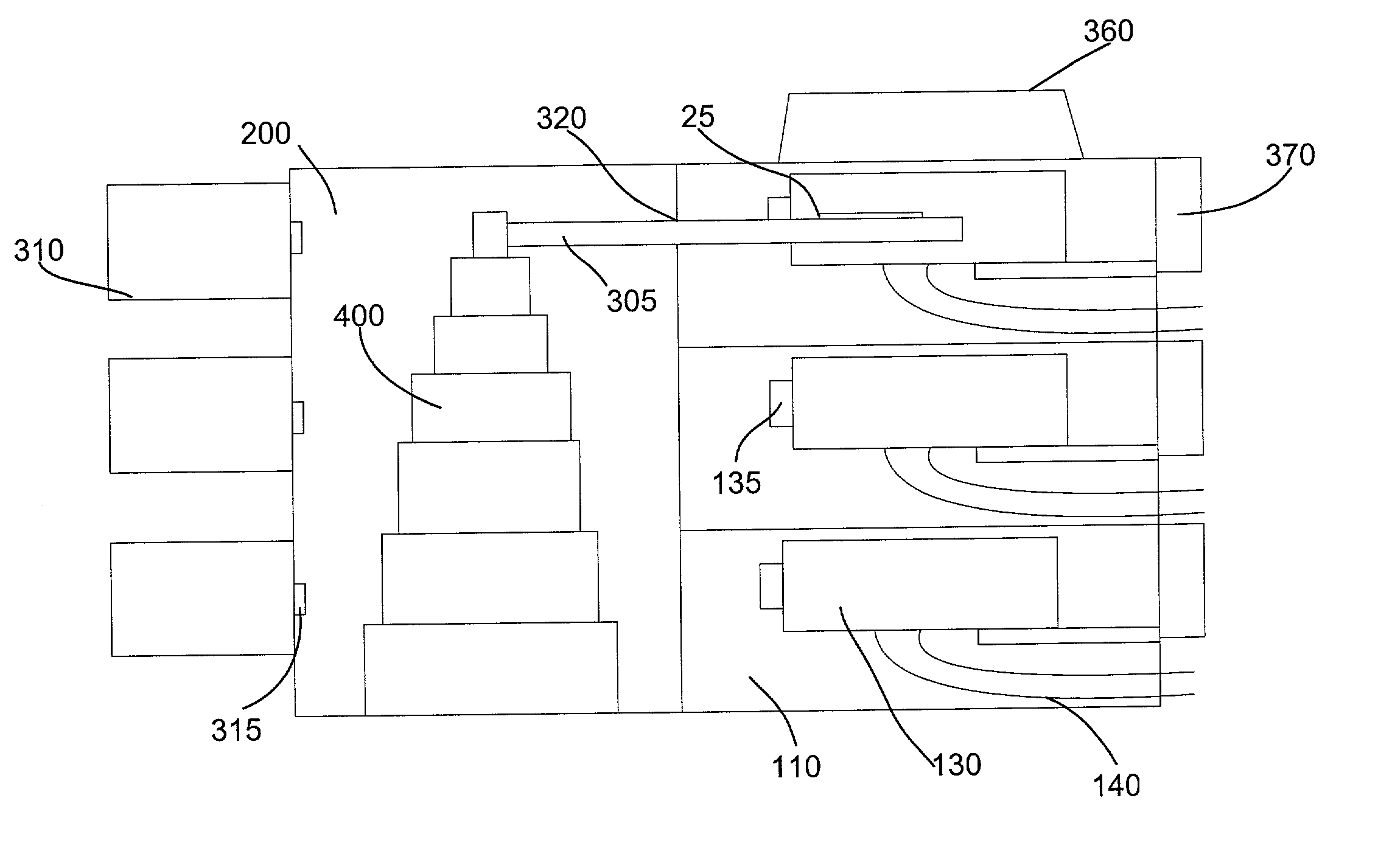
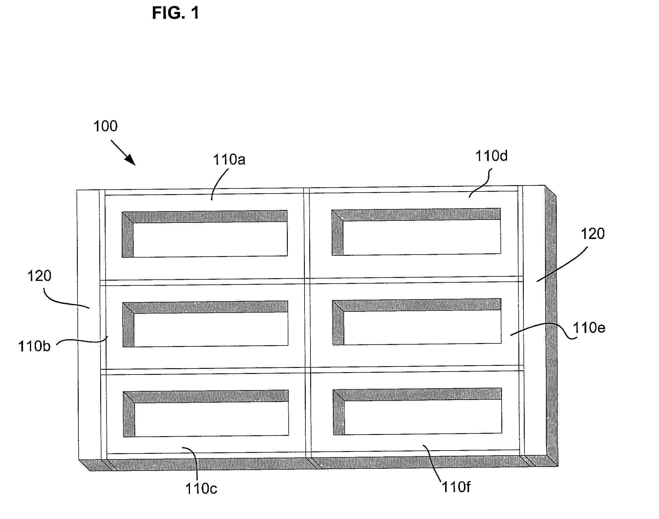
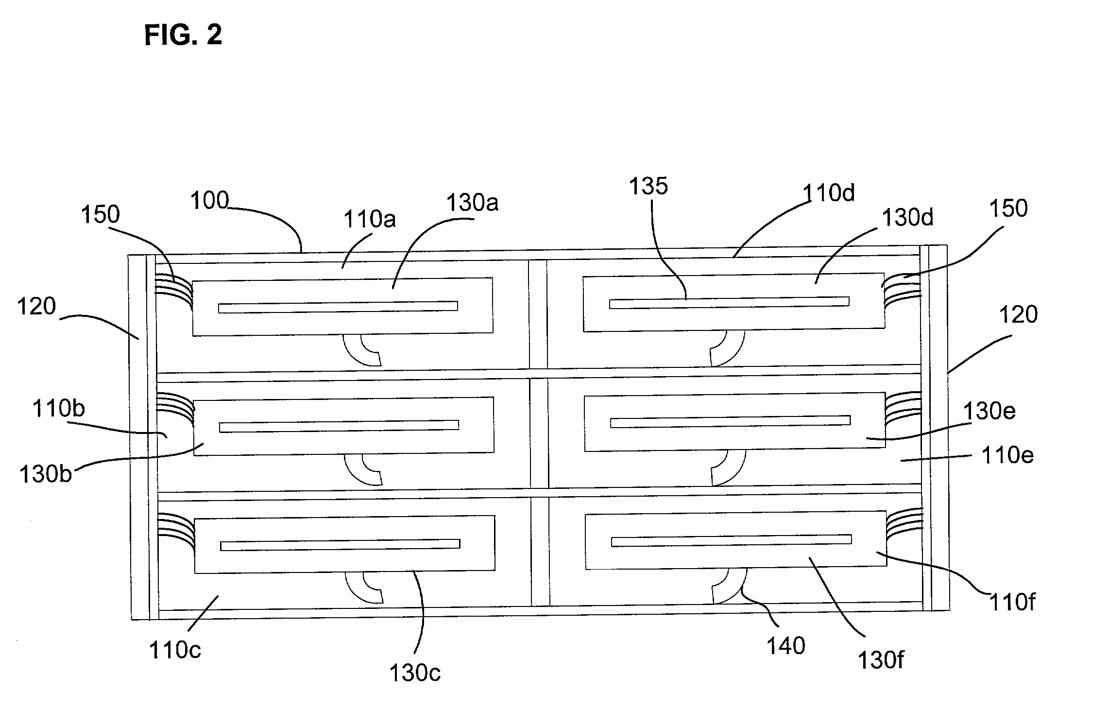
[0007] An integrated workpiece vacuum processing system and method for processing semiconductor workpieces is provided. In one embodiment, the processing system comprises a multiple chamber support unit having a plurality of processing chamber support bays arranged in at least two rows and two columns wherein a vacuum processing chamber module is received in each support bay and a transfer chamber is coupled to the plurality of processing chamber modules. In another embodiment, at least three processing chamber support bays are arranged in one column wherein a vacuum processing chamber module is received in each chamber support bay.

[0008] In another aspect, the processing chamber modules located on the same column perform the same processing step to the workpieces.

[0009] In yet another aspect, the processing chamber modules can be inserted or removed from said processing unit.

[0010] FIG. 1 is a simplified schematic front plan view of a multiple chamber support unit in accordance wit...


PUM

PropertyMeasurementUnit
Structureaaaaaaaaaa
Distributionaaaaaaaaaa

Abstract

An integrated workpiece vacuum processing system for processing semiconductor workpieces is provided using a stacked chamber design. The processing system comprises a multiple chamber support unit having a plurality of processing chamber support bays arranged in rows and columns wherein a vacuum processing chamber module is received in each support bay and a transfer chamber is coupled to the plurality of processing chamber modules.

Description

[0001] 1. Field of the Invention[0002] The present invention relates generally to semiconductor processing systems, and more particularly to multiple chamber semiconductor processing systems.[0003] 2. Description of the Related Art[0004] The present invention is related to a silicon wafer processing system that includes multiple process chambers. However, until recently, the typical available processing reactor systems were single chamber batch-type systems in which the chamber is dedicated to a single type of process such as plasma etching or chemical vapor deposition. These process-dedicated batch-type reactor chambers were designed to provide a high processing throughput for a single process step. Some of these single chamber etcher systems did include an associated vacuum load lock that was used for pre- or post-processing.[0005] Multiple chamber systems are relatively new to the art. An article entitled "Dry Etching Systems: Gearing Up for Larger Wafers", in the October, 1985 i...

Claims


Application Information

Patent Timeline
IPC IPC(8): H01L21/00
CPCH01L21/67178
Inventor DONALDSON, GARY R.WANG, WILLIAM
Owner APPLIED MATERIALS INC
Learn More