Silicon seed crystal and method for producing silicon single crystal
a seed crystal and silicon single crystal technology, applied in the field of silicon single crystal production methods, can solve the problems of insufficient mechanical strength obtained by such a diameter, difficulty in using a seed crystal thickness smaller than the range mentioned above, and serious accident threats
Inactive Publication Date: 2002-07-25
SHIN-ETSU HANDOTAI CO LTD
View PDF0 Cites 2 Cited by
- Summary
- Abstract
- Description
- Claims
- Application Information
AI Technical Summary
Problems solved by technology
In order to safely pull a single crystal ingot while withstanding the weight of heavy single crystal ingot, it is difficult to use a thickness of the seed crystal smaller than the range mentioned above, considering the strength of the material.
The mechanical strength obtained by such a diameter has become insufficient for supporting a single crystal ingot getting heavier with recent use of a larger diameter of the silicon single crystals, and thus a serious accident threatens to occur, for example, the single crystal ingot falls due to breakage of the neck portion of a small diameter.
For the pulling of recent single crystals whose length and diameter are increasingly getting longer and larger, for example, which have a weight of 150 kg or more, the mechanical strength of the neck portion obtained even in these methods may become insufficient, and therefore they cannot be considered ultimate solutions.
Therefore, the applicants of the present application previously developed a method for converting crystals into single crystals without forming a neck portion, which is the most problematic factor as for ensuring the mechanical strength, and filed a patent application therefor (Japanese Patent Application No. 9-17687).
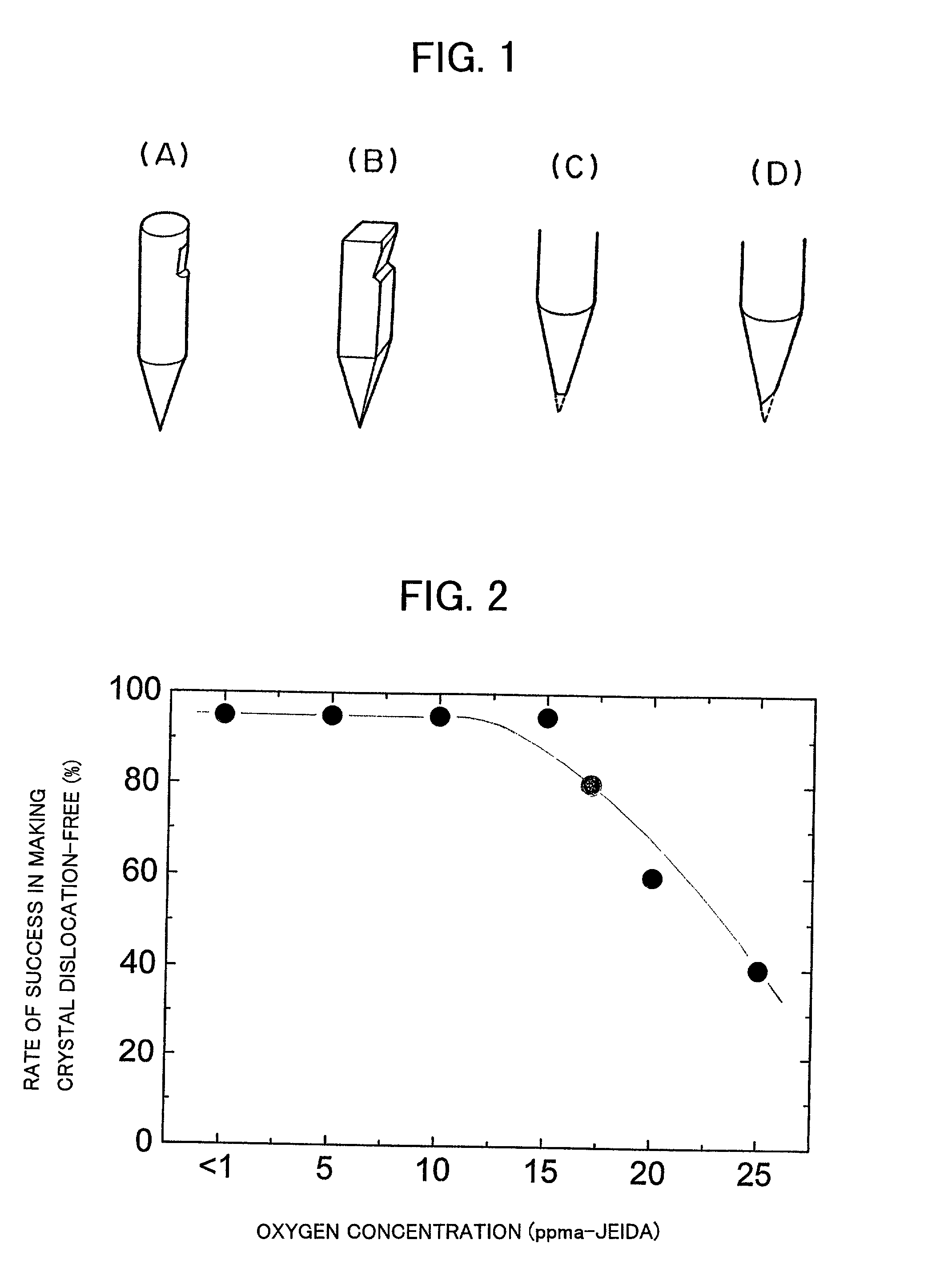
In addition, such conditions do not necessarily afford a high rate of success in making crystals dislocation-free.
However, it is the rate of success in making crystals dislocation-free that may be a difficulty in the dislocation-free seeding method.
That is, according to this method, if dislocations are once introduced, the operation cannot be reattempted unless the seed crystal is changed.
In addition, even though the seeding is performed in a dislocation-free state in this method, slip dislocations may be generated when the seed crystal is left at a temperature around the melting point of silicon for a certain period of time after a predetermined length of the tapered tip end of the seed crystal is melted, or depending on the period requiring for starting the crystal growth, and such dislocations may further increase.
Investigations of the cause of this phenomenon revealed that the control of the factors which had conventionally been controlled,
Method used
View moreImage
Smart ImageViewing Examples


Examples
 PUM
| Property | Measurement | Unit |
|---|---|---|
| Fraction | aaaaa | aaaaa |
| Fraction | aaaaa | aaaaa |
| Fraction | aaaaa | aaaaa |
Abstract
There are disclosed a silicon seed crystal which is composed of silicon single crystal and used for the Czochralski method, wherein oxygen concentration in the seed crystal is 15 ppma (JEIDA) or less, a silicon seed crystal which is used for the Czochralski method, wherein the silicon seed crystal does not have a straight body, and a method for producing a silicon single crystal by the Czochralski method comprising using said seed crystal, bringing a tip end of the seed crystal into contact with a silicon melt to melt the tip end of the seed crystal, with or without performing necking operation, and growing a silicon single crystal. The method is capable of improving the rate of success in making crystals dislocation-free and the productivity of single crystal rods regardless of the use of necking operation.
Description
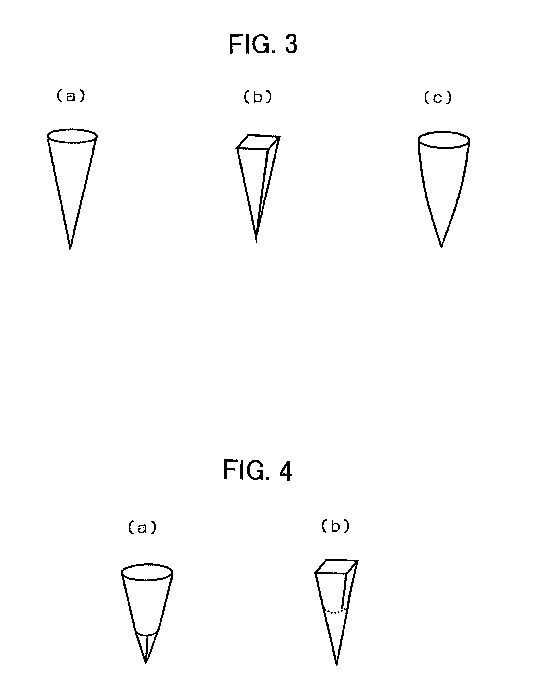
[0001] 1. Field of the Invention[0002] The present invention related to a method for producing a silicon single crystal, wherein the silicon single crystal is grown by the Czochralski method (CZ method) with or without performing necking operation, and a silicon seed crystal.[0003] 2. Related Art[0004] In the conventional production of silicon single crystals according to the CZ method, a silicon single crystal is used as a seed crystal, which is brought into contact with silicon melt and then slowly pulled while being rotated to grow a single crystal ingot. In such a method, after the seed crystal is brought into contact with the silicon melt, the so-called necking is performed to form a neck portion having a smaller diameter of around 3 mm to eliminate dislocation propagated from slip dislocations generated in the seed crystal in high density due to thermal shock, then the diameter of the crystal is increased to a predetermined diameter, and a dislocation-free silicon single cryst...
Claims
Login to View More Application Information
Patent Timeline
 IPC IPC(8): C30B15/00C30B15/36
CPCC30B15/36C30B29/06Y10S117/902Y10S117/911Y10S117/916Y10T428/2982C30B15/00
Inventor IINO, EIICHIKIMURA, MASANORI
Owner SHIN-ETSU HANDOTAI CO LTD
Features
- R&D
- Intellectual Property
- Life Sciences
- Materials
- Tech Scout
- Unparalleled Data Quality
- Higher Quality Content
- 60% Fewer Hallucinations
Learn More Browse by: Latest US Patents, China's latest patents, Technical Efficacy Thesaurus, Application Domain, Technology Topic, Popular Technical Reports.
© 2025 PatSnap. All rights reserved.Legal|Privacy policy|Modern Slavery Act Transparency Statement|Sitemap|About US| Contact US: help@patsnap.com