Vertical electrode structure comprising low-resistance film for preventing damage during etching
a technology of etching and resistance film, which is applied in the direction of semiconductor devices, electrical equipment, radio frequency controlled devices, etc., can solve the problems of increasing manufacturing costs, damage other parts, and deteriorating semiconductor integration density, so as to reduce the restriction on design necessary for avoiding charging damage, suppress transistor characteristics due to charging damage, and reduce design freedom
- Summary
- Abstract
- Description
- Claims
- Application Information
AI Technical Summary
Benefits of technology
Problems solved by technology
Method used
Image
Examples
second embodiment
(B) Second Embodiment
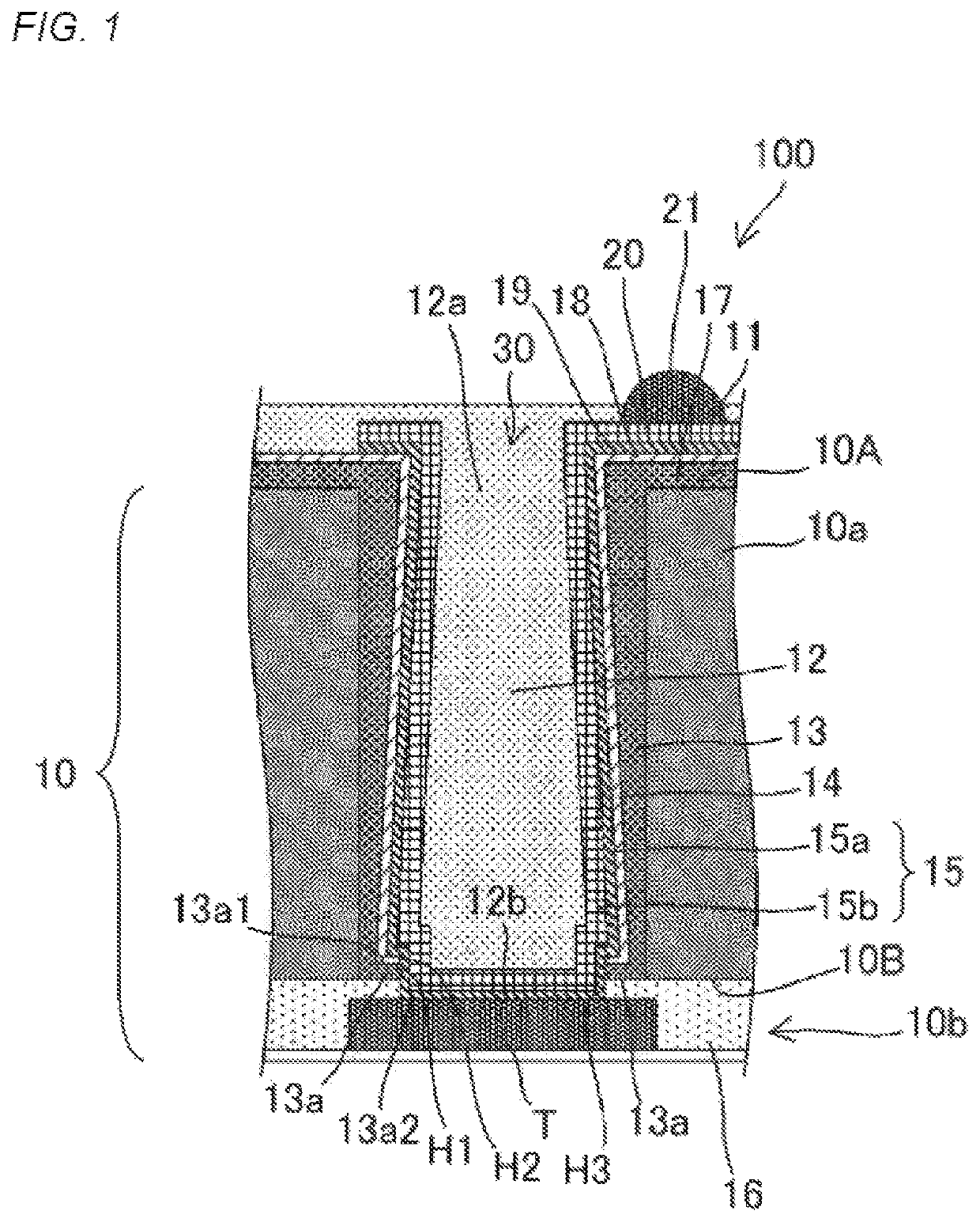
[0079]FIG. 8 is a view illustrating a cross section of a main part of a semiconductor device 200 according to the present embodiment. The semiconductor device 200 has a similar configuration to the above-described semiconductor device 100 except shapes of a low-resistance film and an insulating film in a vicinity of a hole bottom and a barrier metal film and a conductive portion formed on the low-resistance film and the insulating film.
[0080]Therefore, hereinafter, shapes and a method of manufacturing the low-resistance film and the insulating film in the vicinity of the hole bottom and the barrier metal film and the conductive portion formed on the low-resistance film and the insulating film of the semiconductor device 200 will be mainly described and detailed description of other configurations is omitted, and signs are given by adding 2 to the beginning of the signs of the configuration of the semiconductor device 100 as necessary.
[0081]A low-resistance film ...
third embodiment
(C) Third Embodiment
[0091]FIG. 12 is a view illustrating a cross section of a main part of a semiconductor device 300 according to the present embodiment. The semiconductor device 300 has a similar configuration to the above-described semiconductor device 100 except the number of times of stacking of a low-resistance film.
[0092]Therefore, hereinafter, a shape and a manufacturing method regarding stacking of the low-resistance film of the semiconductor device 300 will be mainly described and detailed description of other configurations is omitted, and signs are given by adding 3 to the beginning of the signs of the configuration of the semiconductor device 100 as necessary.
[0093]A low-resistance film 314 of the semiconductor device 300 is similar to the low-resistance film 14 of the semiconductor device 100 in being continuously provided from a vicinity of an opening portion 312a to a vicinity of a hole bottom 312b of a vertical hole 312 inside an insulating film 313.
[0094]The low-re...
fourth embodiment
(D) Fourth Embodiment
[0106]FIG. 18 is a view illustrating a cross section of a main part of a semiconductor device 400 according to the present embodiment. The semiconductor device 400 has a similar configuration to the above-described semiconductor device 100 except an entire shape and a manufacturing method of a low-resistance film.
[0107]Therefore, hereinafter, the entire shape and the manufacturing method of the low-resistance film of the semiconductor device 400 will be mainly described and detailed description of other configurations is omitted, and signs are given by adding 4 to the beginning of the signs of the configuration of the semiconductor device 100 as necessary.
[0108]A low-resistance film 414 of the semiconductor device 400 is similar to the low-resistance film 14 of the semiconductor device 100 in being continuously provided from a vicinity of an opening portion 412a to a vicinity of a hole bottom 412b of a vertical hole 412 inside an insulating film 413.
[0109]An ins...
PUM
| Property | Measurement | Unit |
|---|---|---|
| diameter | aaaaa | aaaaa |
| aspect ratio | aaaaa | aaaaa |
| aspect ratio | aaaaa | aaaaa |
Abstract
Description
Claims
Application Information
 - R&D Engineer
- R&D Manager
- IP Professional
- Industry Leading Data Capabilities
- Powerful AI technology
- Patent DNA Extraction
Browse by: Latest US Patents, China's latest patents, Technical Efficacy Thesaurus, Application Domain, Technology Topic, Popular Technical Reports.
© 2024 PatSnap. All rights reserved.Legal|Privacy policy|Modern Slavery Act Transparency Statement|Sitemap|About US| Contact US: help@patsnap.com


