
Organic compound, organic light emitting diode including the same, and organic light emitting display

a light-emitting diode and organic compound technology, applied in organic chemistry, solid-state devices, semiconductor devices, etc., can solve the problems of reducing increasing the size of the display, so as to prevent deterioration or deformation, improve the lifespan of the organic light-emitting diode, and good thermal stability

Active Publication Date: 2022-02-22
LG DISPLAY CO LTD
View PDF40 Cites 0 Cited by
  • Summary
  • Abstract
  • Description
  • Claims
  • Application Information

AI Technical Summary

Benefits of technology

[0010]It is an aspect of the present disclosure to provide an organic compound which has good electron injection / electron transport characteristics while exhibiting high thermal stability.
[0011]It is another aspect of the present disclosure to provide an organic light emitting diode which has reduced driving voltage while exhibiting improved emission performance and lifespan, and an organic light emitting display including the same.
[0023]An organic compound according to the present disclosure has a phenanthroline moiety substituted with at least one aromatic ring. Since the organic compound has a high decomposition temperature or a high glass transition temperature to exhibit good thermal stability due to the presence of the aromatic ring-substituted phenanthroline moiety, the organic compound is prevented from being deteriorated or degraded by Joule's heat generated upon operation thereof. Accordingly, when used in an organic light emitting diode, the organic compound can improve lifespan of the organic light emitting diode while reducing driving voltage thereof.
[0024]In addition, since the phenanthroline moiety of the organic compound has a nitrogen atom having a sp2 hybrid orbital, which is relatively rich in electrons, the organic compound has good electron transport properties. Thus, the organic compound can be used as a material for an electron transport layer. In particular, the nitrogen atom of the phenanthroline moiety is bonded to an alkali metal or alkali earth metal compound, which is a dopant for an N-type charge generation layer, to form a gap state. As a result, a difference in energy level between the N-type charge generation layer and a P-type charge generation layer is reduced, thereby facilitating injection of electrons into the N-type charge generation layer while maximizing transfer of electrons from the N-type charge generation layer to an adjacent electron transport layer.
[0025]Namely, use of the organic compound in the N-type charge generation layer of the organic light emitting diode or the organic light emitting display allows efficient transfer of electrons from the N-type charge generation layer to the electron transport layer.
[0026]Further, since the organic compound containing nitrogen atoms is combined with the alkali metal or alkali earth metal compound in the N-type charge generation layer, the alkali metal or alkali earth metal compound can be prevented from diffusing into the P-type charge generation layer. As a result, deterioration in lifespan of the organic light emitting diode can be prevented.

Problems solved by technology

Recently, there is increasing interest in flat display elements occupying a small space, with increasing size of displays.
In such a charge generation layer used in a typical tandem OLED, due to a difference in energy level between the N-type charge generation layer and the P-type charge generation layer, charges are generated at an interface between the P-type charge generation layer and an adjacent hole injection layer or hole transport layer, causing deterioration in electron injection into the N-type charge generation layer.
When the N-type charge generation layer is doped with a metal, the metal is likely to diffuse into the P-type charge generation layer, causing reduction in lifespan of the OLED.
Particularly, a typical material for charge generation layers does not have sufficient thermal / electrical stability.
Accordingly, long-term operation of the white OLED causes the material for charge generation layers to be degraded or deteriorated.
As a result, not only efficiency in electron injection from the interface between the P-type charge generation layer and the adjacent hole injection layer or hole transport layer into the N-type charge generation layer but also efficiency in electron injection from the N-type charge generation layer into an adjacent electron transport layer can be greatly reduced, causing reduction in performance and lifespan of the OLED.

Method used


Image

  • Organic compound, organic light emitting diode including the same, and organic light emitting display
  • Organic compound, organic light emitting diode including the same, and organic light emitting display
  • Organic compound, organic light emitting diode including the same, and organic light emitting display

Examples


experimental example 1

Evaluation of Thermal Stability and Electron Transfer Properties

[0211]Each of the organic compounds prepared in Preparative Examples 1 to 6 and Comparative Preparative Examples 1 to 6 was evaluated as to thermal stability and electron transfer properties. In thermal analysis, thermogravimetric analysis (TGA) and differential scanning calorimetry (DSC) were carried out to determine the decomposition temperature (1%, 5%) and glass transition temperature (Tg) of each organic compound, respectively. In evaluation of electron transfer properties, electron affinity (EA), electron reorganization energy (λelectron), and electron / hole rate constant ratio (ket(e) / ket(h)) of each organic compound were calculated based on density functional theory (B3LYP / 6-31G*). Results are shown in Table 1.

[0212]

TABLE 1Thermal analysis(° C.)Simulation analysisTaTaElectron(1%)(5%)Taaffinityλelectronket(e) / ket(h)EN-m0023924431210.620.250.70EN-m002-13684281120.470.290.79EN-m0054124571150.600.260.28EN-m005-138742...

example 1

Fabrication of Tandem Organic Light Emitting Diode

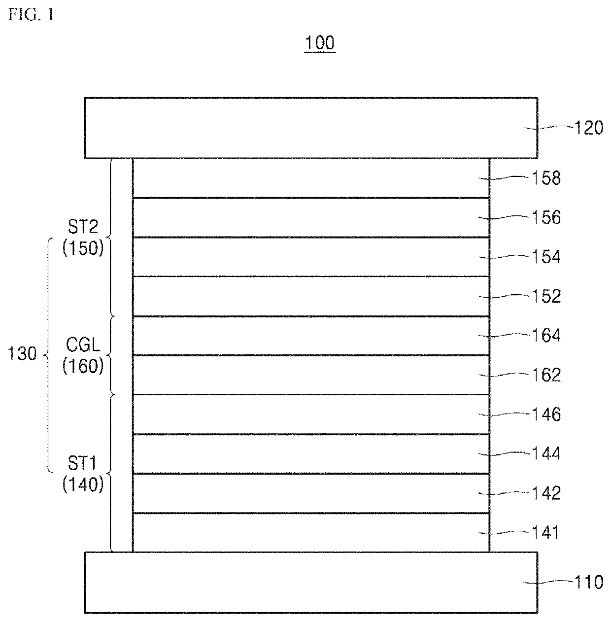
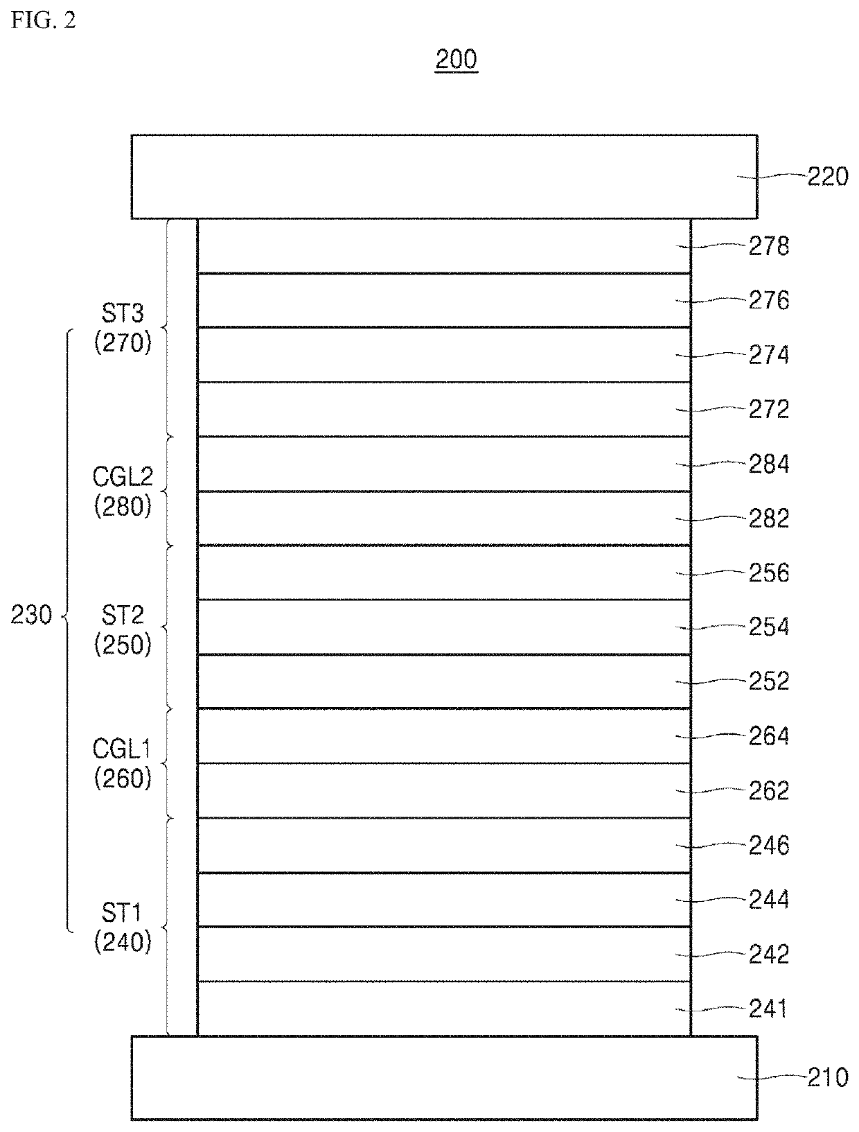
[0214]In a vacuum chamber at a pressure of 5×10⁻⁸ to 7×10⁻⁸ torr, a tandem organic light emitting diode was fabricated by sequentially depositing the following layers on an indium-tin-oxide (ITO) substrate:

[0215]A hole injection layer (NPD-based host doped with 10 wt % of F4-TCNQ; 100 Å), a first hole transport layer (NPD-based compound; 1200 Å), a first light emitting material layer (blue light emitting material layer; anthracene-based host doped with 4 wt % of pyrene dopant; 200 Å), a first electron transport layer (1,3,5-tri[(3-pyridyl)-phen-3-yl]benzene (TmPyPB)-based compound; 100 Å), a first N-type charge generation layer (EN-m002 doped with 2 wt % of Li; 100 Å), a first P-type charge generation layer (NPD-based host doped with 10 wt % of F4-TCNQ; 200 Å), a second hole transport layer (NPD-based compound; 200 Å), a second light emitting material layer (yellow light emitting material layer; CBP-based host doped with Ir complex; ...

example 2

Fabrication of Tandem Organic Light Emitting Diode

[0217]A tandem organic light emitting diode was fabricated in the same manner as in Example 1 except that, as a host for the first and second N-type charge generation layers, EN-m005 prepared in Preparative Example 2 was used instead of EN-m002.


PUM

PropertyMeasurementUnit
thicknessaaaaaaaaaa
thicknessaaaaaaaaaa
thicknessaaaaaaaaaa

Abstract

Disclosed herein is an organic compound, an organic light emitting diode including the same, and an organic light emitting display. The organic compound according to the present disclosure is a phenanthroline compound represented by the following Formula 1, which is used as an electron transport material of an organic light emitting diode. The phenanthroline compound can increase lifespan of the organic light emitting diode while reducing driving voltage of the organic light emitting diode.

Description

BACKGROUNDTechnical Field[0001]The present disclosure relates to an organic compound for charge generation layer and / or electron transport materials, an organic light emitting diode including the same, and an organic light emitting display including the same.Description of the Related Art[0002]Recently, there is increasing interest in flat display elements occupying a small space, with increasing size of displays. A technology of an organic light emitting display including organic light emitting diodes (OLEDs) as the flat display elements has been rapidly developed in the art.[0003]An OLED emits light through annihilation of pairs of holes and electrons created upon injection of holes and electrons from a hole injection electrode (anode) and an electron injection electrode (cathode) into a light emitting material layer (EML) interposed between the anode and the cathode. Advantageously, such an OLED is formed on a flexible transparent substrate, such as plastic, is operable at a low ...

Claims


Application Information

Patent Timeline
Patent Type & Authority Patents(United States)
IPC IPC(8): H01L51/00C07D471/04H01L27/32H01L51/50H01L51/52
CPCH01L51/0072C07D471/04H01L27/322H01L27/3209H01L27/3244H01L51/5016H01L51/5044H01L51/5072H01L51/5278H10K59/32H10K59/38H10K59/12H10K50/16H10K50/19H10K85/654H10K85/657H10K50/13H10K50/14H10K50/805H10K85/6572H10K50/11H10K50/131H10K2101/10
Inventor SHIN, JICHEOLYOO, SEONKEUNYOON, SEUNGHEE
Owner LG DISPLAY CO LTD
Learn More