
Method for producing an output coupling element for an optoelectronic component and output coupling element

an optoelectronic component and output coupling element technology, applied in the direction of luminescent compositions, semiconductor devices, chemistry apparatus and processes, etc., can solve the problems of limited indium phosphide quantum dots, etc., and achieve the effect of efficiently and simply producing an output coupling elemen

Active Publication Date: 2021-08-24
OSRAM OLED
View PDF15 Cites 0 Cited by
  • Summary
  • Abstract
  • Description
  • Claims
  • Application Information

AI Technical Summary

Benefits of technology

[0005]Embodiments provide a method for producing an output coupling element for an optoelectronic component that efficiently and simply produces an efficient output coupling element. Further embodiments provide an output coupling element for an optoelectronic component.
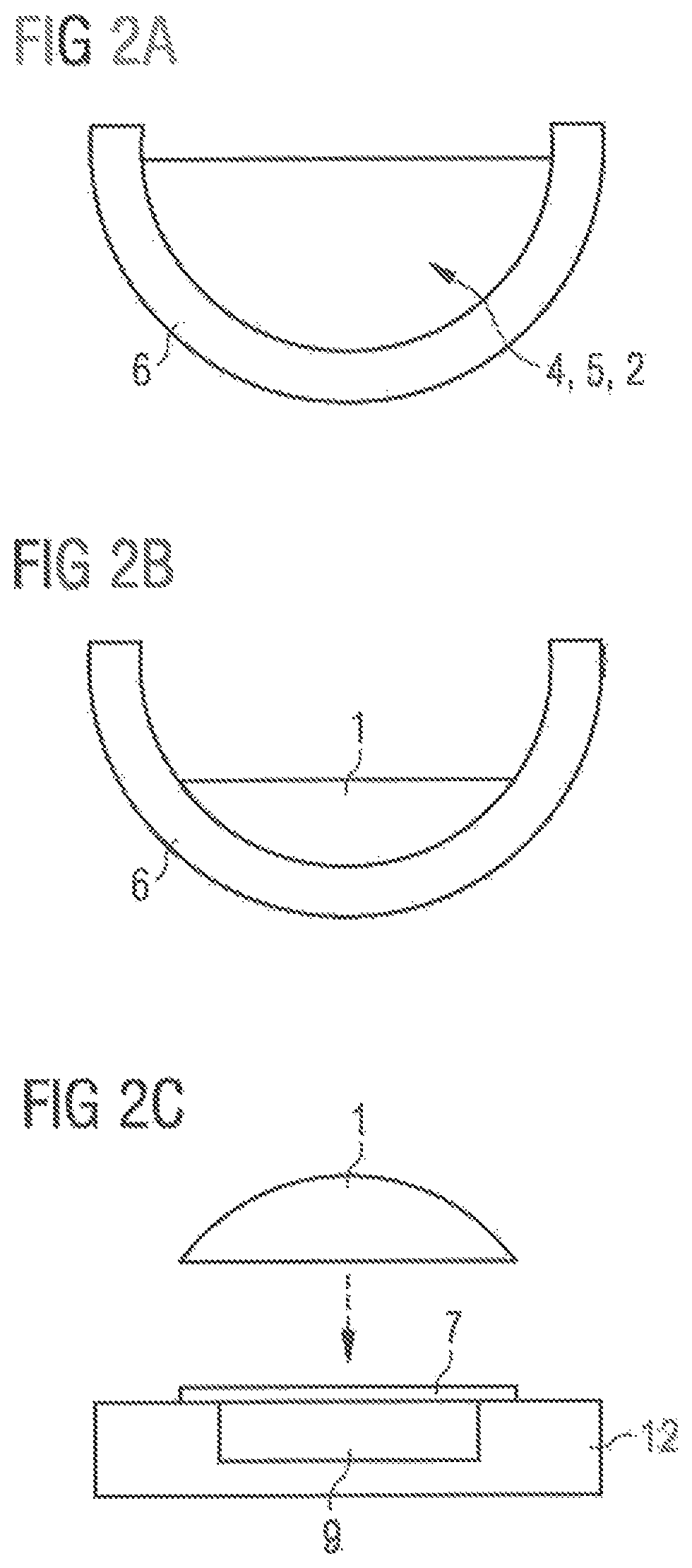
[0033]According to at least one embodiment, the surface of the carrier is non-stick coated. This is advantageous because the output coupling element can thus easily be removed from the carrier. Alternatively or additionally, the surface of the optoelectronic component is non-stick coated.
[0036]The inventor has recognized that the use of an output coupling element described here can provide an optoelectronic component that has an increased decoupling, for example, from the semiconductor layer sequence and / or from the conversion element. The output coupling element is formed matrix-free, i.e., it preferably only has the quantum dots. The output coupling element is highly refractive and can easily be applied to a surface of an optoelectronic component, in particular a light-emitting diode.

Problems solved by technology

Indium phosphide quantum dots would therefore be limited for the use of IR diodes with a wavelength of 950 nm.

Method used


Image

  • Method for producing an output coupling element for an optoelectronic component and output coupling element
  • Method for producing an output coupling element for an optoelectronic component and output coupling element
  • Method for producing an output coupling element for an optoelectronic component and output coupling element

Examples


Embodiment Construction

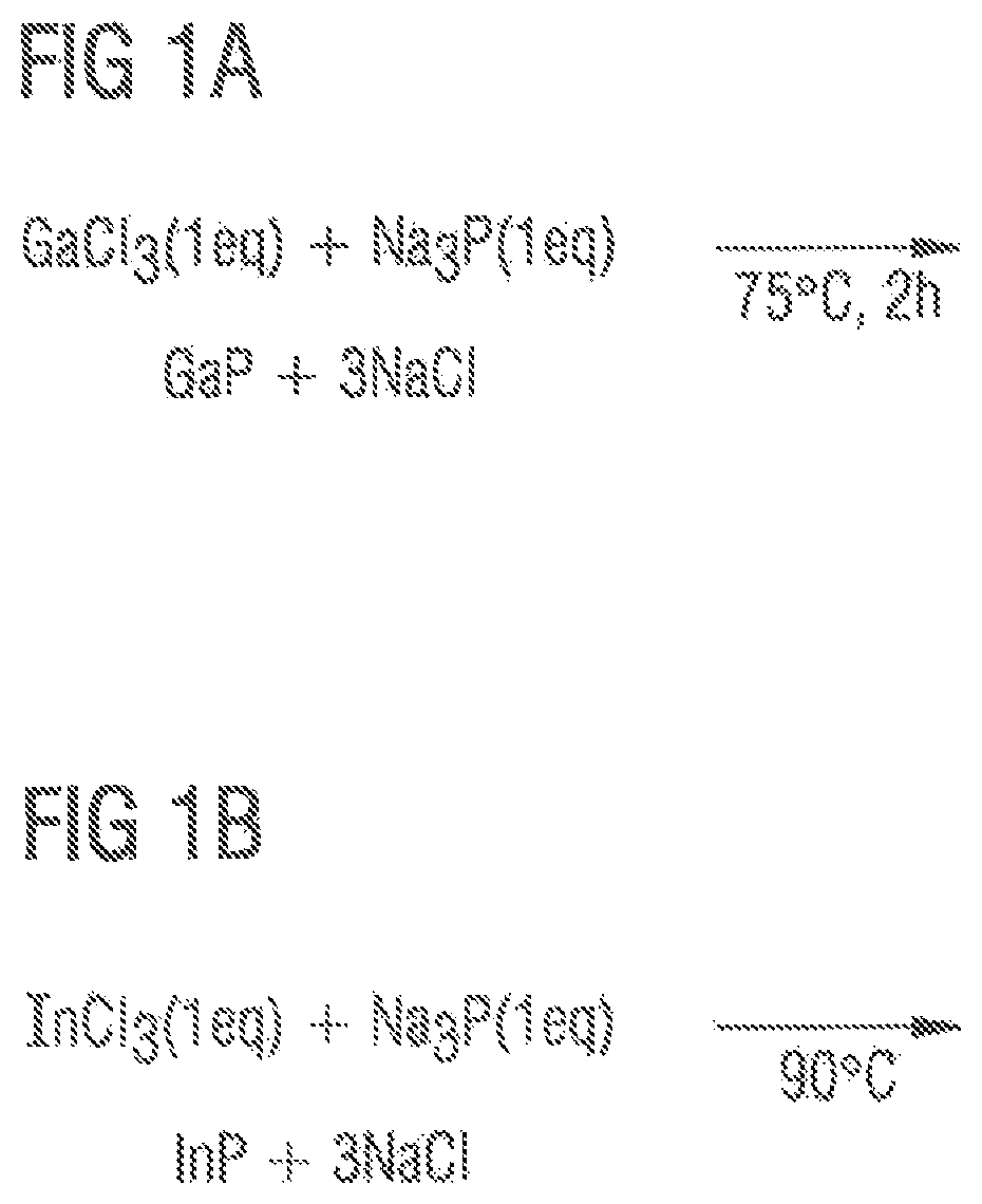
lass="d_n">[0045]FIG. 1A shows a possible synthesis for the production of an output coupling element according to an embodiment. For example, gallium chloride, which is commercially available, can be boiled in the same ratio with sodium phosphide at 75° C. for two hours in benzene under argon reflux until gallium phosphide and sodium chloride are produced. Gallium phosphide can be dried and stored under argon. Sodium chloride can be extracted with water. Accordingly, as shown in FIG. 1B, indium phosphide can also be produced from indium chloride and sodium phosphide. Alternatively, other gallium or indium halides can be used to produce gallium or indium phosphide.

[0046]Alternatively, other alkali phosphides can also be used to produce gallium or indium phosphide. Indium phosphide is boiled in xylene under argon reflux at higher temperatures of 90° C., for example.

[0047]Dimethylformamide (DMF) can also be used as a suspension medium instead of benzene or xylene. The suspension medium...


PUM

PropertyMeasurementUnit
refractive indexaaaaaaaaaa
wavelengthsaaaaaaaaaa
wavelengthaaaaaaaaaa

Abstract

A method for producing an output coupling element and an output coupling element are disclosed. In an embodiment a method includes producing a suspension having quantum dots in a suspension medium, wherein each quantum dot comprises a core having a semiconductor material, directly applying the suspension onto a surface of an optoelectronic component and / or onto a surface of a carrier and removing the suspension medium for producing the output coupling element, wherein the output coupling element is matrix-free and transparent to radiation of a red range and / or a IR range.

Description

[0001]This patent application is a national phase filing under section 371 of PCT / EP2018 / 052280, filed Jan. 30, 2018, which claims the priority of German patent application 102017102477.8, filed Feb. 8, 2017, each of which is incorporated herein by reference in its entirety.TECHNICAL FIELD[0002]The invention relates to a method of producing an output coupling element for an optoelectronic component. Furthermore, the invention relates to an output coupling element, in particular for an optoelectronic component.BACKGROUND[0003]The output coupling elements described previously exhibit insufficient decoupling of light generated in a semiconductor chip of an optoelectronic component, since there are large refractive index differences at the interface between the semiconductor chip surface and its surroundings. This problem is particularly relevant for semiconductor chips that emit radiation of the red or IR wavelength range and have InGaAlP- and / or GaAs-based materials with a high refrac...

Claims


Application Information

Patent Timeline
Patent Type & Authority Patents(United States)
IPC IPC(8): H01L33/50H01L33/58C09K11/08C09K11/70
CPCH01L33/502C09K11/0883C09K11/70H01L33/58H01L2933/0041H01L2933/0058H01L33/44H01L2933/0025H10K50/858H10K2102/331
Inventor DIRSCHERL, GEORG
Owner OSRAM OLED
Learn More