Electro-optical device and electronic apparatus
a technology of optical devices and electronic devices, applied in the direction of dielectric characteristics, instruments, other printed circuit details, etc., can solve the problems of difficult to appropriately provide mold material between the first wiring substrate and the second wiring substrate, and it is not possible to confirm whether or not the non-cured mold material is provided
- Summary
- Abstract
- Description
- Claims
- Application Information
AI Technical Summary
Benefits of technology
Problems solved by technology
Method used
Image

Examples
first exemplary embodiment
[0019]Basic Configuration
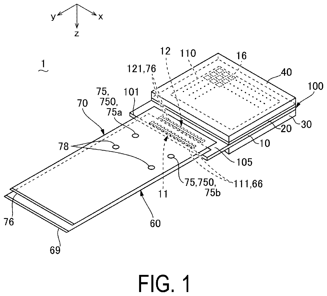
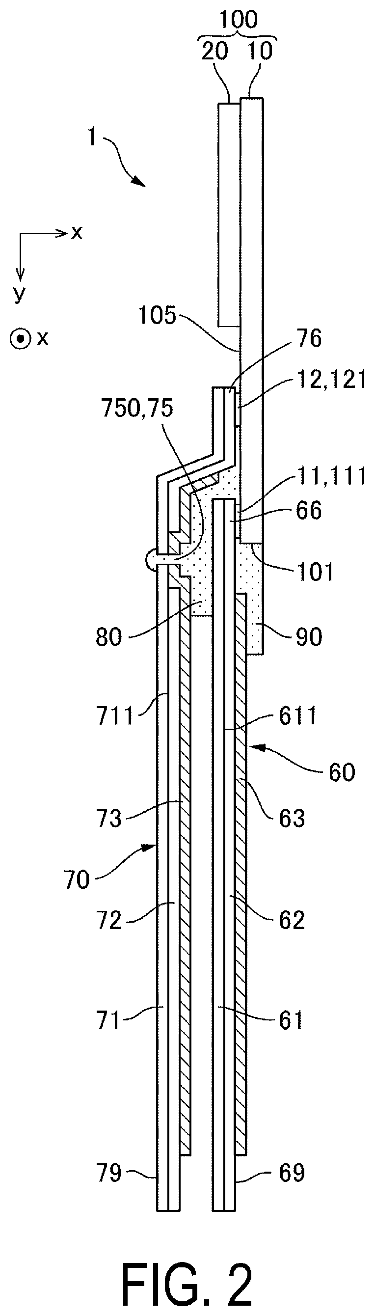
[0020]FIG. 1 is a perspective view illustrating a mode of the electro-optical device 1 according to a first exemplary embodiment of the present disclosure. FIG. 2 is an explanatory diagram schematically illustrating a cross-section of the electro-optical device 1 illustrated in FIG. 1, and corresponds to a cross-sectional view taken along a dotted line A-A′ in FIG. 3A, which will be described below. Note that in FIG. 2, a seal material, an electro-optical layer, a first dust-proof glass 30, a second dust-proof glass 40, and the like are not illustrated.
[0021]In FIG. 1 and FIG. 2, the electro-optical device 1 is a liquid crystal device used as a light valve or the like, which will be described below, and includes a liquid crystal panel that is an electro-optical panel 100. In the electro-optical panel 1, a counter substrate 20 on which a common electrode (not illustrated) and the like are formed is bonded, using the seal material (not illustrated), to an elec...
second exemplary embodiment
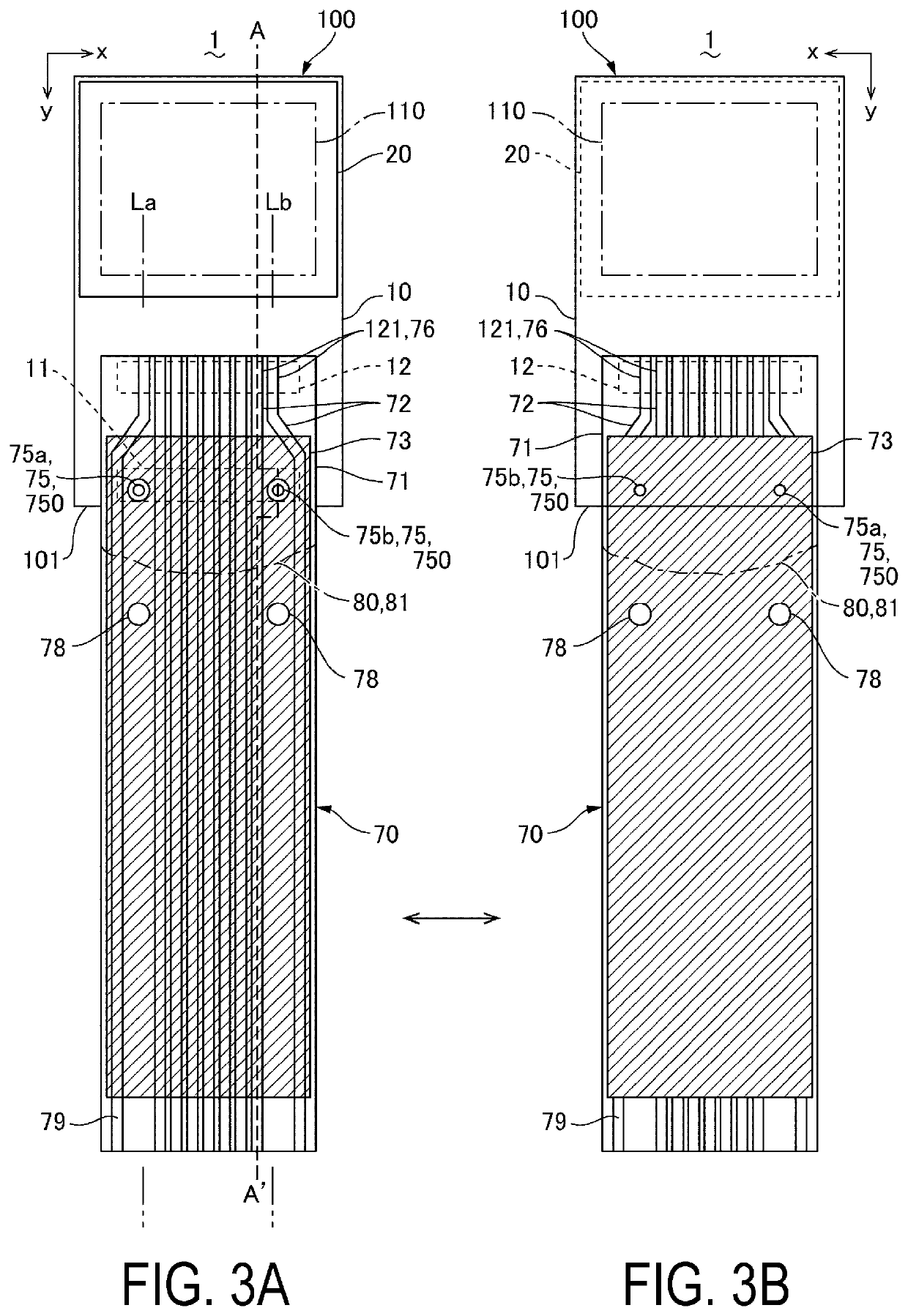
[0049]FIGS. 4A and 4B are explanatory diagrams of the electro-optical device 1 according to a second embodiment of the present disclosure. FIG. 4A illustrates a plan view of the second wiring substrate 70 and the like as viewed from the counter substrate 20 side, and FIG. 4B is a bottom surface view of the second wiring substrate 70 and the like as viewed from the electro-optical device substrate 10 side. In FIGS. 4A and 4B, the illustration of the first wiring substrate 60 is omitted. Further, in FIGS. 4A and 4B, of the second wiring substrate 70, visible portions are indicated by solid lines. Note that a basic configuration of the present exemplary embodiment is the same as that of the first exemplary embodiment, and thus, common portions will be denoted by the same reference signs and descriptions thereof will be omitted.
[0050]As illustrated in FIGS. 4A and 4B, similarly to the first exemplary embodiment, in the present exemplary embodiment also, the light-transmission windows 75...
third exemplary embodiment
[0054]FIGS. 5A and 5B are explanatory diagrams of the electro-optical device 1 according to a third exemplary embodiment of the present disclosure. FIG. 5A illustrates a plan view of the second wiring substrate 70 and the like as viewed from the counter substrate 20 side, and FIG. 5B is a bottom surface view of the second wiring substrate 70 and the like as viewed from the electro-optical device substrate 10 side. In FIGS. 5A and 5B, the illustration of the first wiring substrate 60 is omitted. Further, in FIGS. 5A and 5B, visible portions of the second wiring substrate 70 are indicated by solid lines. Note that a basic configuration of the present exemplary embodiment is the same as that of the first exemplary embodiment, and thus, common portions will be denoted by the same reference signs and descriptions thereof will be omitted.
[0055]As illustrated in FIGS. 5A and 5B, similarly to the first exemplary embodiment, also in the present exemplary embodiment, the light-transmission wi...
PUM
| Property | Measurement | Unit |
|---|---|---|
| diameter | aaaaa | aaaaa |
| diameter | aaaaa | aaaaa |
| flexible | aaaaa | aaaaa |
Abstract
Description
Claims
Application Information
 - R&D
- Intellectual Property
- Life Sciences
- Materials
- Tech Scout
- Unparalleled Data Quality
- Higher Quality Content
- 60% Fewer Hallucinations
Browse by: Latest US Patents, China's latest patents, Technical Efficacy Thesaurus, Application Domain, Technology Topic, Popular Technical Reports.
© 2025 PatSnap. All rights reserved.Legal|Privacy policy|Modern Slavery Act Transparency Statement|Sitemap|About US| Contact US: help@patsnap.com