Chip package and chip thereof

a chip and chip technology, applied in the field of chip packages, can solve the problems of less bonding area of electrodes on the chip, and the difficulty of electrodes on the led to be electrically connected to the substrate, so as to avoid electrical connection failure and facilitate electrical connection

Active Publication Date: 2020-10-06
CHIPBOND TECH
View PDF27 Cites 0 Cited by
  • Summary
  • Abstract
  • Description
  • Claims
  • Application Information

AI Technical Summary

Benefits of technology

[0009]The present invention utilizes the first confining wall of the first electrode to confine at least one conductive particle of the adhesive in the first confining groove. For this reason, the first conductive particle is unable to be moved with the adhesive when bonding the chip to the substrate, and the first electrode of the chip is able to be electrically connected to the first bonding pad of the substrate via the first conductive particle in the first confining groove. The present invention can avoid the electrical connection failure between the chip and the substrate, such as to facilitate electrical connection of micro LED.

Problems solved by technology

However, the smaller the chip, the smaller the bonding area of electrodes on the chip.
Especially, if the chip is a micro LED, the electrodes on the LED are more difficult to be electrically connected to the substrate.

Method used


Image

  • Chip package and chip thereof
  • Chip package and chip thereof
  • Chip package and chip thereof

Examples


Embodiment Construction

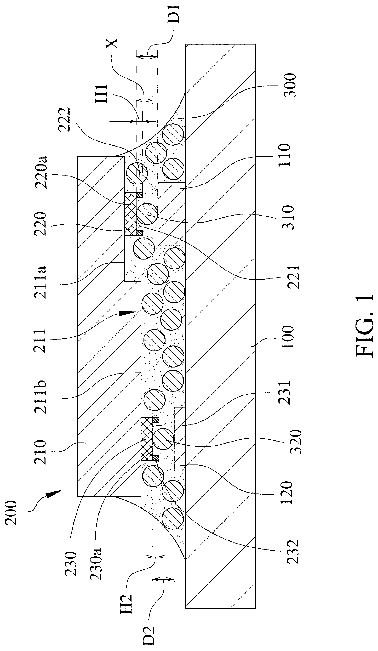
[0014]With reference to FIG. 1, a chip package of the present invention includes a substrate 100, a chip 200 and an adhesive 300. The chip 200 is, but not limit to, a LED chip.

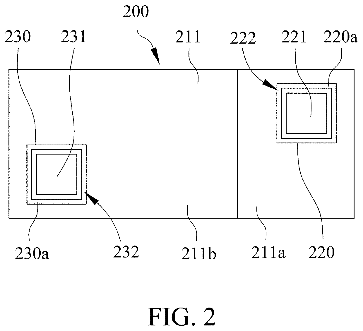
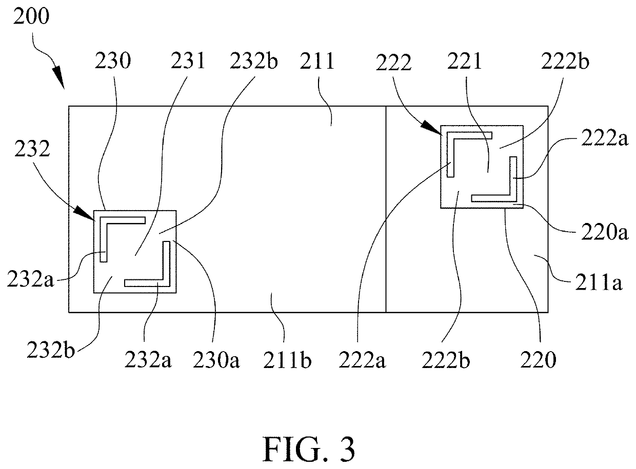
[0015]With reference to FIGS. 1 and 2, the substrate 100 includes a first bonding pad 110 and a second bonding pad 120, and the chip 200 includes a body 210, a first electrode 220 and a second electrode 230. The first electrode 220 and the second electrode 230 are disposed and exposed on a surface 211 of the body 210. The first electrode 220 includes a first exposed surface 220a, a first confining groove 221 and a first confining wall 222 which is peripherally located around the first confining groove 221. The second electrode 230 includes a second exposed surface 230a, a second confining groove 231 and a second confining wall 232 which is peripherally located around the second confining groove 231.

[0016]With reference to FIGS. 1 and 2, the first confining wall 222 and the second confining wall 232 may be made...


PUM

PropertyMeasurementUnit
heightaaaaaaaaaa
heightaaaaaaaaaa
heightaaaaaaaaaa

Abstract

A microchip is electrically connected to a substrate to become a chip package, preferably for LED. A chip of the package includes a body and at least one electrode which is disposed and exposed on a surface of the body. The electrode includes a confining groove and a confining wall. The confining wall is peripherally located around the confining groove and provided to confine at least one conductive particle of an adhesive in the confining groove. The electrode of the chip is electrically connected to a bonding pad of a substrate via the conductive particle confined in the confining groove.

Description

FIELD OF THE INVENTION[0001]This invention relates to a chip package, and more particularly relates to a package for micro LED.BACKGROUND OF THE INVENTION[0002]In conventional technique, a chip is electrically connected to a substrate by using a conductive adhesive having conductive particles. However, the smaller the chip, the smaller the bonding area of electrodes on the chip.[0003]During bonding of the chip to the substrate, resin in the heated conductive adhesive is flowable such that the conductive particles may flow with the resin.[0004]If the conductive particles flowing with the resin are not confined between an electrode of the chip and a bonding pad of the substrate result from the bonding area of the electrodes on the chip is reduced, the chip is unable to be electrically connected to the substrate via the conductive particles after solidifying the resin. Especially, if the chip is a micro LED, the electrodes on the LED are more difficult to be electrically connected to t...

Claims


Application Information

Patent Timeline
Patent Type & Authority Patents(United States)
IPC IPC(8): H01L33/62H01L33/38
CPCH01L33/38H01L33/62H01L33/54H01L24/29H01L2224/05557H01L2933/0066H01L2224/06102H01L2224/05568H01L2224/02175H01L2224/02185H01L2224/0219H01L2224/056H01L2224/2929H01L2224/293H01L2224/83851H01L2224/83203H01L2224/04026H01L24/32H01L24/05H01L24/06H01L24/83H01L2224/05554H01L2224/83101H01L2924/06H01L2924/00014H01L24/26H01L23/13
Inventor HSIEH, CHIN-TANGSHIH, CHENG-HUNG
Owner CHIPBOND TECH
Why Eureka
Try Eureka