Apparatus and method for measurement of multilayer structures
a multi-layer structure and measurement method technology, applied in the direction of phase-affecting property measurement, measurement devices, instruments, etc., can solve the problems of destroying the measurement procedure used in zobel '417, tedious, and one material at a time, and none of the above methods can both non-destructively determine the number of layers in the multi-layer structur
- Summary
- Abstract
- Description
- Claims
- Application Information
AI Technical Summary
Benefits of technology
Problems solved by technology
Method used
Image
Examples
first embodiment
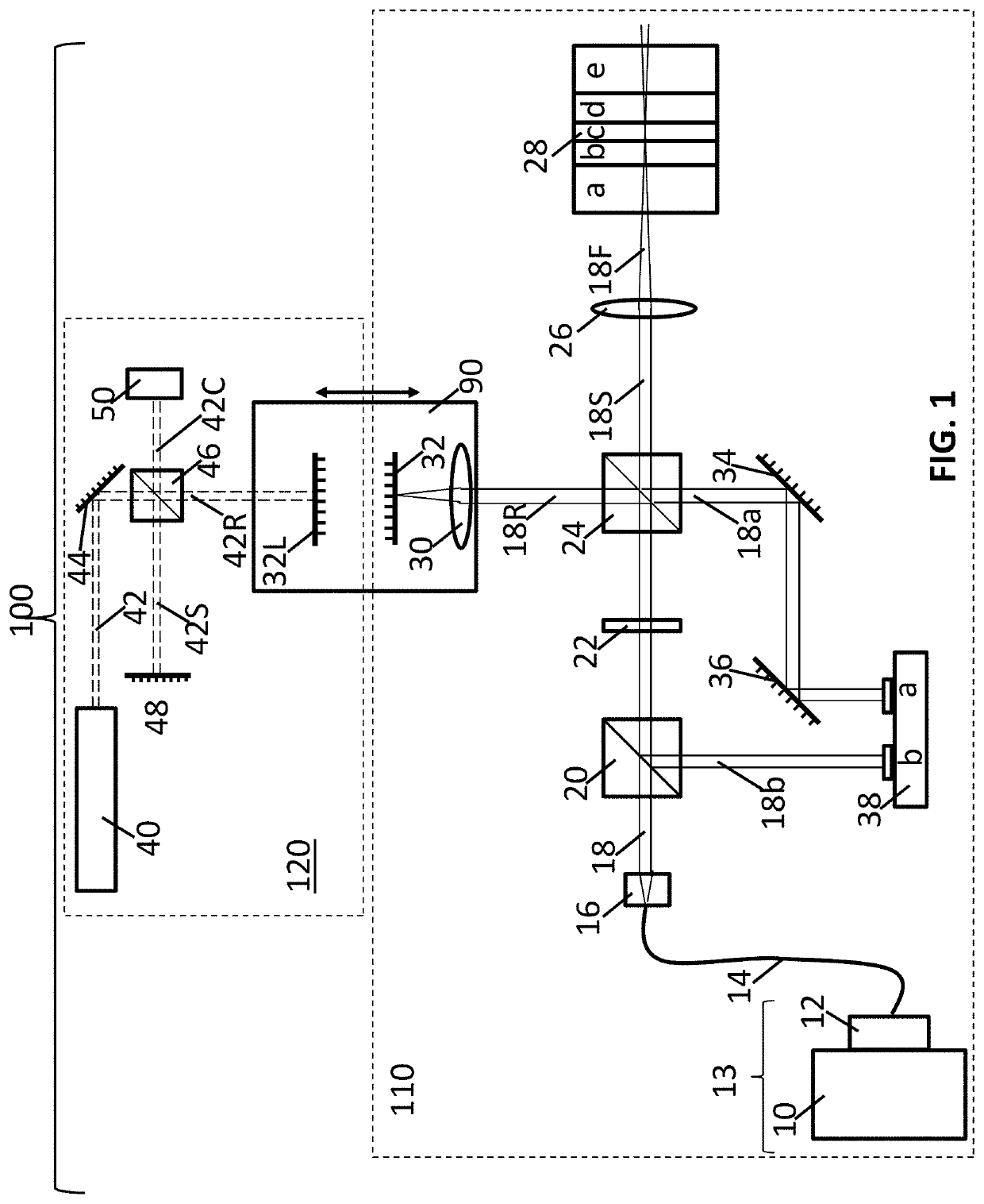
[0044]Turning now to FIG. 1, a schematic of an interferometer apparatus 100 used to measure the optical thickness of each of the layers in a multilayer structure 28 as a function of wavelength is shown. The interferometer apparatus 100 is a dual interferometer comprising a free-space low-coherence interferometer 110 (shown in the lower dashed rectangle) and a laser interferometer 120 (shown in the upper dashed rectangle). The two interferometers share a common variable optical path delay element 90 as described in Marcus '409. The laser interferometer 120 continuously measures the displacement of the reference path and is used to provide an accurate distance scale for the low-coherence interferometer as described in Marcus '409.
[0045]As shown in FIG. 1, the light source of the free space low-coherence interferometer 110 is a broadband low-coherence light source 10, and preferably a supercontinuum light source such as an NKT Photonics EXW-12 Supercontinuum light source (SCLS) which e...
second embodiment
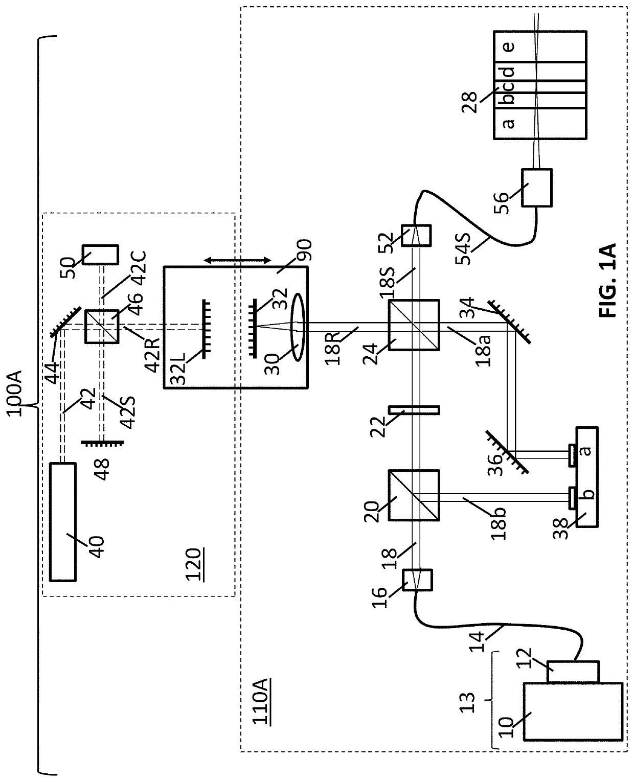
[0049]FIG. 1A shows a schematic of an interferometer apparatus 100A used to measure the optical thickness of each of the layers in a multilayer structure 28 as a function of wavelength. Most of the components of interferometer apparatus 100 and 100A are the same, and all components of the laser interferometer 120 are the same in both embodiments. The only differences in the components between low-coherence interferometer 110A and low-coherence interferometer 110 occur in the sample arm of the low-coherence interferometer 110A. The focusing lens 26 is replaced with a fiber collimator 52 which is used to couple the incident light portion of sample arm collimated beam 18S into a sample arm optical fiber 54S which is then input into an optical probe 56 which focuses light onto the multilayer structure 28. Part of the light that is focused on the multilayer structure 28 through optical probe 56 reflects off each optical interface of the multilayer structure 28 back through optical probe ...
third embodiment
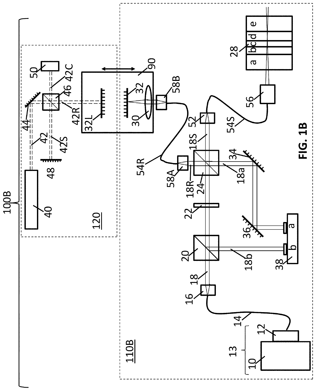
[0050]FIG. 1B shows a dual interferometer apparatus 100B used to measure the optical thickness of each of the layers in a multilayer structure 28 as a function of wavelength. Most of the components of dual interferometer apparatus 100A and 100B are the same, and all components of the laser interferometer 120 are the same in both embodiments. The only differences in the components between low-coherence interferometer 110A and low-coherence interferometer 110B occur in the reference arm of the low-coherence interferometer 110B. Instead of the incident light portion of reference arm collimated beam 18R being directly incident on the reference arm lens 30 as shown in FIG. 1 and FIG. 1A, the incident light portion of reference arm collimated beam 18R shown in FIG. 1B part of the collimated beam 18R region is coupled into a fiber collimator 58A and transmitted through optical fiber 54R and coupled into a second fiber collimator 58B before being incident on reference arm lens 30 which then...
PUM
| Property | Measurement | Unit |
|---|---|---|
| coherence length | aaaaa | aaaaa |
| optical thickness | aaaaa | aaaaa |
| physical thickness | aaaaa | aaaaa |
Abstract
Description
Claims
Application Information
 - R&D
- Intellectual Property
- Life Sciences
- Materials
- Tech Scout
- Unparalleled Data Quality
- Higher Quality Content
- 60% Fewer Hallucinations
Browse by: Latest US Patents, China's latest patents, Technical Efficacy Thesaurus, Application Domain, Technology Topic, Popular Technical Reports.
© 2025 PatSnap. All rights reserved.Legal|Privacy policy|Modern Slavery Act Transparency Statement|Sitemap|About US| Contact US: help@patsnap.com


