Photoelectric conversion device, manufacturing method thereof, and apparatus

a technology manufacturing method, which is applied in the direction of diodes, semiconductor devices, radiation controlled devices, etc., can solve the problems of boron readily trapped in silicon oxide film, inability to perform high-temperature thermal processing aimed at crystal defect recovery in this manufacturing process, and impaired sensor characteristics of photoelectric conversion device, etc., to improve the sensor characteristics of a photoelectric conversion device, improve the effect of temperatur

Active Publication Date: 2020-06-16
CANON KK
View PDF60 Cites 1 Cited by
  • Summary
  • Abstract
  • Description
  • Claims
  • Application Information

AI Technical Summary

Benefits of technology

[0003]The micropatterning process advances lowering of the temperature in the manufacturing process of a photoelectric conversion device. High-temperature thermal processing aimed at crystal defect recovery cannot be performed in this manufacturing process, so boron is doped near the surface of a semiconductor substrate. Boron is readily trapped in the silicon oxide film, and the sensor characteristics of the photoelectric conversion device are impaired (for example, a white spot and a dark current increase). An aspect of the present invention provides a technique for improving the sensor characteristics of a photoelectric conversion device.

Problems solved by technology

High-temperature thermal processing aimed at crystal defect recovery cannot be performed in this manufacturing process, so boron is doped near the surface of a semiconductor substrate.
Boron is readily trapped in the silicon oxide film, and the sensor characteristics of the photoelectric conversion device are impaired (for example, a white spot and a dark current increase).

Method used


Image

  • Photoelectric conversion device, manufacturing method thereof, and apparatus
  • Photoelectric conversion device, manufacturing method thereof, and apparatus
  • Photoelectric conversion device, manufacturing method thereof, and apparatus

Examples


Embodiment Construction

[0011]Embodiments of the present invention will now be described with reference to the accompanying drawings. The same reference numerals denote the same parts throughout various embodiments and a repetitive description thereof will be omitted. Embodiments can be properly changed and combined.

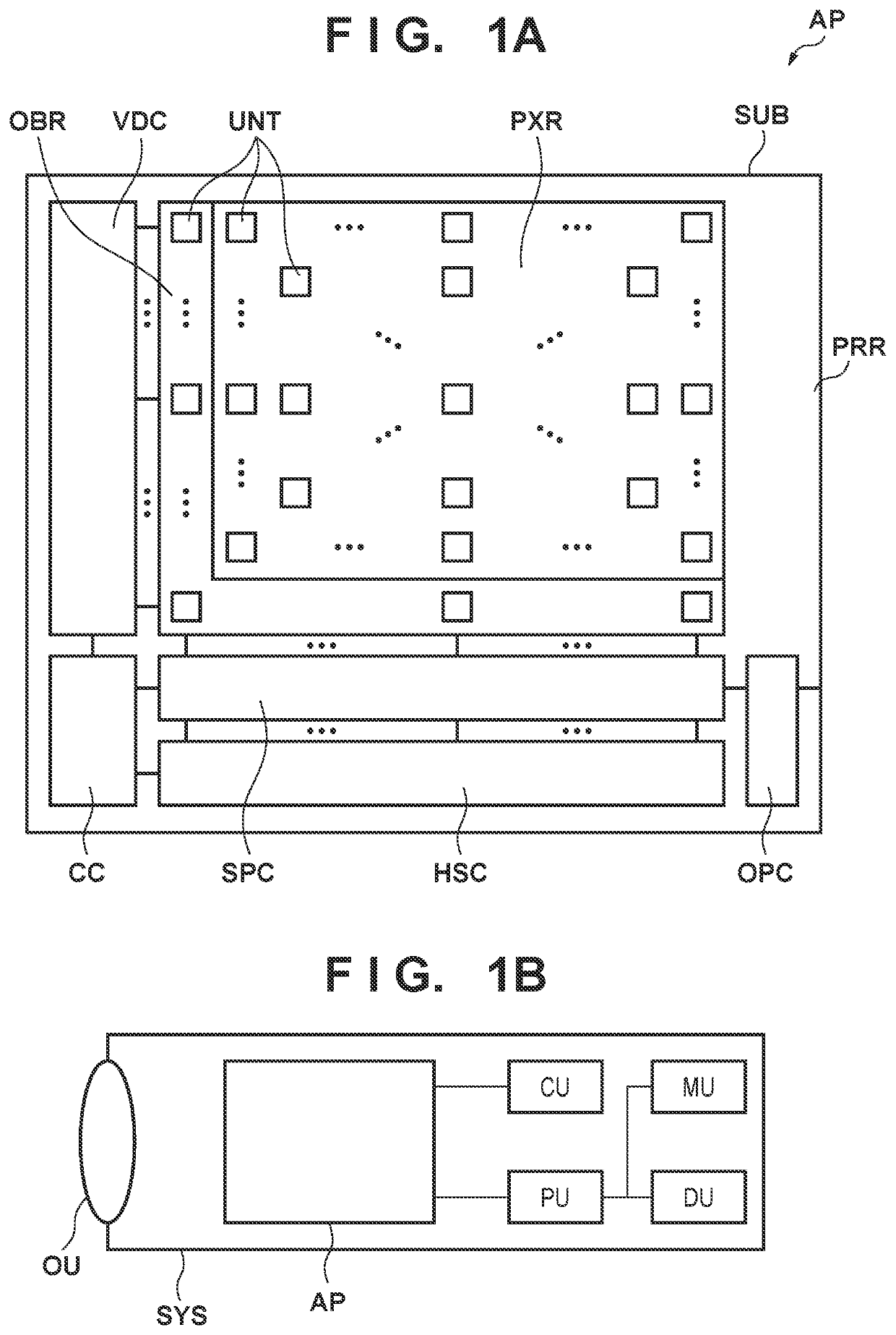
[0012]An example of the arrangement of a photoelectric conversion device AP according to some embodiments will be described with reference to FIG. 1A. The photoelectric conversion device AP may also be called a solid-state photoelectric conversion device. The arrangement of the photoelectric conversion device AP may be an existing one and an example of the arrangement will be explained simply below. The photoelectric conversion device AP is constituted by forming various circuits on a semiconductor substrate SUB. The photoelectric conversion device AP may be mounted in a package.

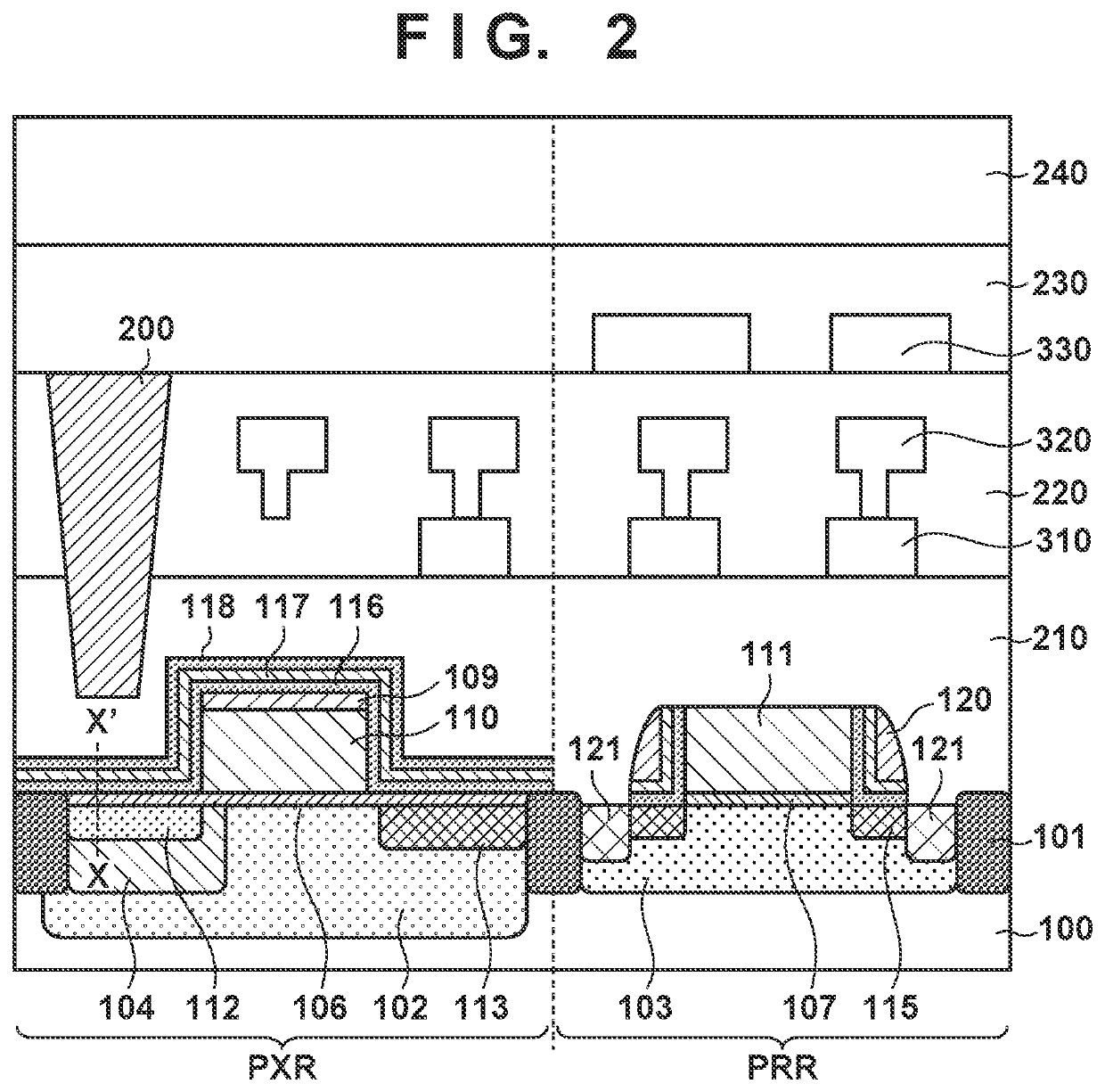
[0013]The semiconductor substrate SUB includes a pixel region PXR, an optical black region OBR, and a peripheral circ...


PUM

PropertyMeasurementUnit
distanceaaaaaaaaaa
temperatureaaaaaaaaaa

Abstract

A photoelectric conversion device comprises a semiconductor substrate including a photoelectric conversion portion, a silicon oxide film arranged above the photoelectric conversion portion, and an insulating film arranged between the photoelectric conversion portion and the silicon oxide film. An n-type first impurity region constituting part of the photoelectric conversion portion and a p-type second impurity region arranged between the insulating film and the first impurity region are provided in the semiconductor substrate. A portion of the insulating film above the second impurity region, and the second impurity region contain boron. An integrated value of a boron concentration from the surface of the semiconductor substrate to a first position where a boron concentration takes a minimal value in the second impurity region is larger than that from the surface of the semiconductor substrate to an upper surface of the silicon oxide film.

Description

BACKGROUND OF THE INVENTIONField of the Invention[0001]The present invention relates to a photoelectric conversion device, a manufacturing method thereof, and an apparatus.Description of the Related Art[0002]In a solid-state photoelectric conversion device, a p-type impurity region containing an impurity such as boron is formed in the surface region of a photoelectric conversion portion in order to suppress a white spot or a dark current arising from an interface state or a crystal defect. When the p-type impurity region is formed from boron in the surface region of the photoelectric conversion portion, boron may be trapped in an insulating film such as a silicon oxide film covering the photoelectric conversion portion owing to thermal diffusion or the like. Japanese Patent Laid-Open No. 2007-208052 proposes a method of forming a diffusion barrier layer such as a silicon nitride film between a photoelectric conversion portion and a silicon oxide film.SUMMARY OF THE INVENTION[0003]Th...

Claims


Application Information

Patent Timeline
Patent Type & Authority Patents(United States)
IPC IPC(8): H01L31/0264H01L31/0352H01L31/0232H01L27/146H01L31/036H01L31/18
CPCH01L27/14689H01L31/035272H01L31/18H01L31/0264H01L27/14698H01L31/02327H01L31/036H01L27/1461H01L27/14643
Inventor ENDO, NOBUYUKI
Owner CANON KK
Why Eureka
Try Eureka