
Method of manufacturing quantum dot having tunable and narrow light emission wavelength for achieving high color purity and a method of manufacturing film

a manufacturing method and quantum dot technology, applied in the field of quantum dots, can solve the problems of difficult mass-production of inp quantum dots, hardly secured uniformity of particle size, and difficult inp quantum dots, and achieve the effect of wide light emission line width and high color purity

Active Publication Date: 2020-03-03
DAEGU GYEONGBUK INST OF SCI & TECH
View PDF10 Cites 2 Cited by
  • Summary
  • Abstract
  • Description
  • Claims
  • Application Information

AI Technical Summary

Benefits of technology

The technical effect of this patent is to provide a method for manufacturing quantum dots with a narrower light emission wavelength, to achieve high color purity. This is done by tuning the absorption characteristics of the quantum dot core and eliminating the use of zinc precursors during the shell formation process. This method also allows for the manufacturing of a film with the desired quantum dots.

Problems solved by technology

However, InP quantum dots have a disadvantage that it is not only difficult to mass-produce InP quantum dots since the synthesis thereof is generally difficult but also the uniformity of particle size is more hardly secured and the quantum yield (QY) is lower as compared with the existing CdSe quantum dot material.
However, problems such as productivity (reaction time), manufacturing cost and environment (amount of sample, odor, and the like), and securement of coating uniformity are required to be sufficiently considered even when coating the shell.

Method used


Image

  • Method of manufacturing quantum dot having tunable and narrow light emission wavelength for achieving high color purity and a method of manufacturing film
  • Method of manufacturing quantum dot having tunable and narrow light emission wavelength for achieving high color purity and a method of manufacturing film
  • Method of manufacturing quantum dot having tunable and narrow light emission wavelength for achieving high color purity and a method of manufacturing film

Examples


preparation example 1

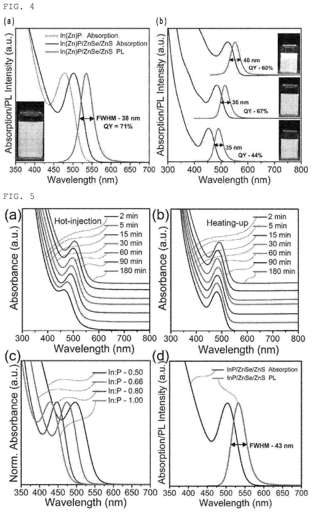
[0136]In(Zn)P / ZnSe / ZnS QDs Emitting at 535 nm (FWHM—38 nm)

[0137]1) 0.15 mmol of indium acetate, 0.075 mmol of zinc acetate, and 0.585 mmol of palmitic acid were mixed with 10 mL of ODE in a 50 mL three-necked flask and the flask was fixed to a Schlenk line by using a reflux condenser.

[0138]2) The mixture was heated at 120° C. for 12 hours in a vacuum state (vacuum level reaching 150 mTorr).

[0139]3) The flask was refilled with N2 and cooled to room temperature. At this point, the mixture turned into a white turbid solution.

[0140]4) A solution containing 0.1 mmol of (TMS)3P and 1 mL of TOP (trioctylphosphine) was injected into the flask. After the injection, the mixture was heated to 305° C. and held at this temperature for 20 minutes.

[0141]5) 0.15 mL of TOP-Se in 0.1 mL of TOP was injected into the flask and the mixture was held at 300° C. for 15 minutes.

[0142]6) 0.1 mmol of zinc stearate in 1 mL of ODE was injected into the flask.

[0143]7) After the state was held for 10 minutes, 0.1...

preparation example 2

[0150]Preparation of In(Zn)P / ZnS QDs Emitting at 488 nm (FWHM—35 nm)

[0151]In(Zn)P / ZnS QDs were prepared in the same manner as in Preparation Example 1 except that (TMS)3 was used by 0.1205 mmol (35 μl) instead of 0.1 mmol and TOP-S was used instead of TOP-Se.

preparation example 3

[0152]Preparation of In(Zn)P / ZnSe / ZnS QDs Emitting at 515 nm (FWHM—36 nm)

[0153]In(Zn)P / ZnSe / ZnS QDs were prepared in the same manner as in Preparation Example 1 except that palmitic acid was used by 0.525 mmol instead of 0.575 mmol.


PUM

PropertyMeasurementUnit
temperatureaaaaaaaaaa
sizeaaaaaaaaaa

Abstract

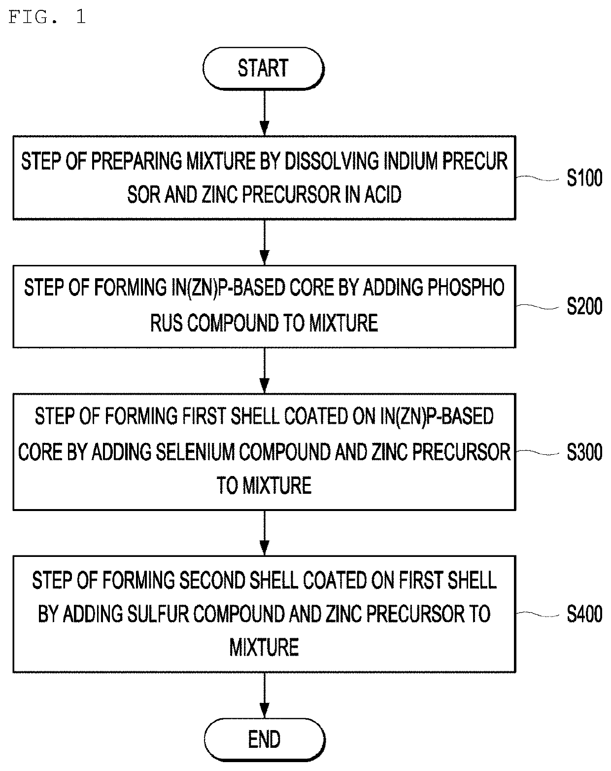
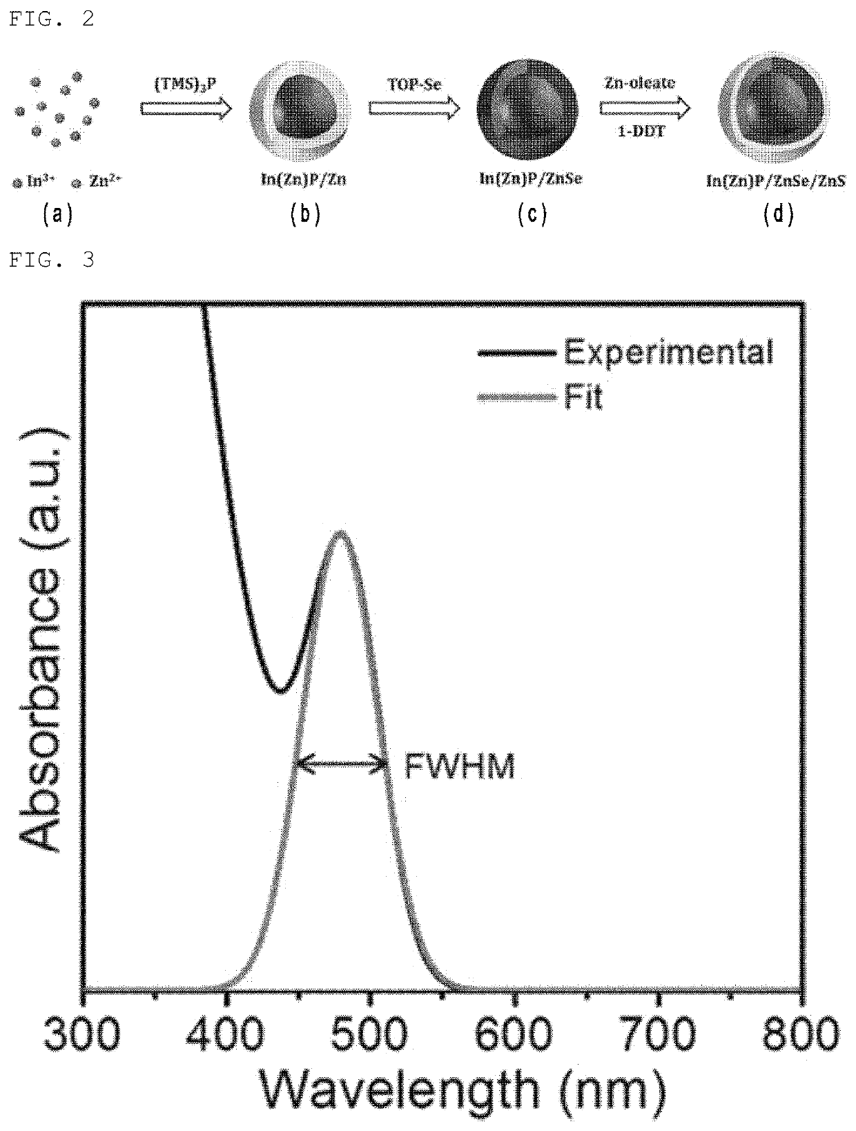
The present disclosure relates to a method of manufacturing a quantum dot having a tunable and narrow light emission wavelength for achieving a high color purity, which for example includes preparing a mixture by dissolving an indium precursor and a zinc precursor in an acid, forming an In(Zn)P-based core by adding a phosphorus compound to the mixture, forming a first shell coated on the In(Zn)P-based core by adding a selenium compound and the zinc precursor to the mixture, and forming a second shell coated on the first shell by adding a sulfur compound and the zinc precursor to the mixture and in which the first shell is formed of ZnSe and the second shell is formed of ZnS.

Description

CROSS-REFERENCE TO RELATED APPLICATION[0001]This application claims priority to and the benefit of Korean Patent Application No. 10-2017-0079391, filed on Jun. 22, 2017 and No. 10-2017-0175583, filed on Dec. 19, 2017, the disclosure of which is incorporated herein by reference in its entirety.BACKGROUND OF THE INVENTION[0002]Field of the Invention[0003]The present invention relates to a quantum dot, and more particularly, to a method of manufacturing a quantum dot having a tunable and narrow light emission wavelength for achieving a high color purity and a method of manufacturing a film.[0004]Description of the Related Art[0005]Quantum dots (QDs) are semiconducting nano-sized particles having a three-dimensionally limited size and exhibit excellent optical and electrical characteristics that are not possessed by semiconducting materials in a bulk state. For example, the color of light emitted from quantum dots may vary depending on the particle size although the quantum dots are pro...

Claims


Application Information

Patent Timeline
Patent Type & Authority Patents(United States)
IPC IPC(8): H01L51/50C09K11/02C09K11/56B82Y30/00B82Y40/00B82Y20/00
CPCH01L51/502C09K11/02C09K11/565B82Y40/00B82Y20/00B82Y30/00H10K50/115
Inventor LEE, JONG SOORAMASAMY, PARTHIBAN
Owner DAEGU GYEONGBUK INST OF SCI & TECH
Learn More