Semiconductor device, liquid discharge head, and liquid discharge apparatus
a liquid discharge head and semiconductor technology, applied in printing and other directions, can solve the problems of upsizing of semiconductor devices, achieve the effects of improving discharge accuracy, increasing the number of pads and lines, and increasing the number of test heaters
- Summary
- Abstract
- Description
- Claims
- Application Information
AI Technical Summary
Benefits of technology
Problems solved by technology
Method used
Image

Examples
first embodiment
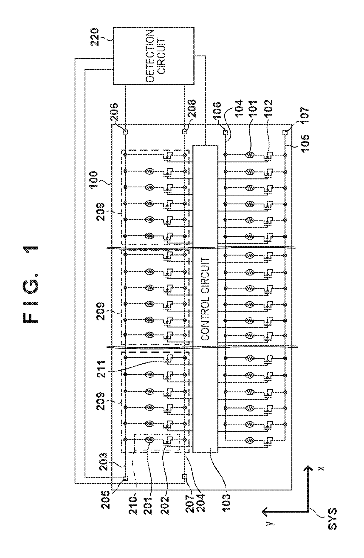
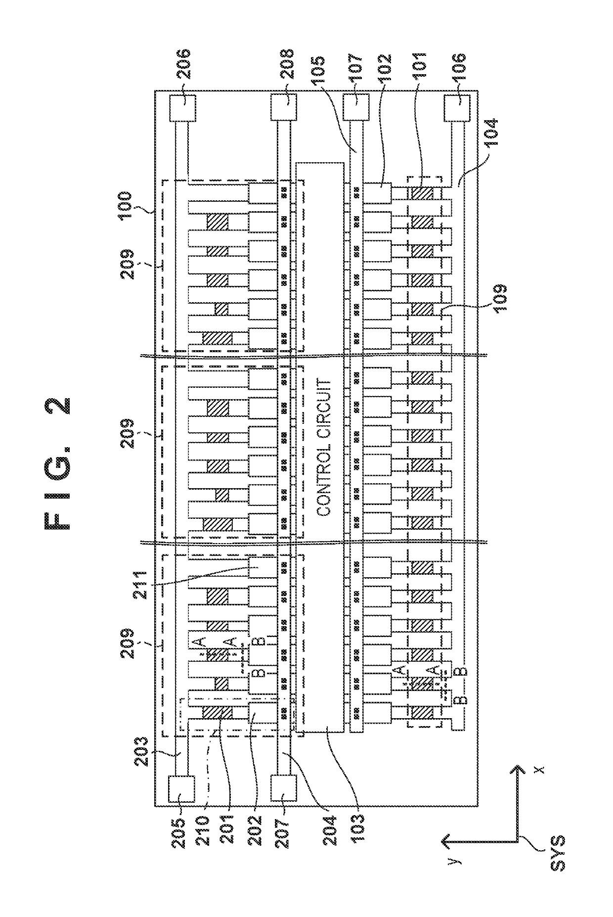
[0013]The arrangement of a semiconductor device 100 will be described with reference to a circuit diagram of FIG. 1. In order to describe directions, a coordinate system SYS along the surface of the semiconductor device 100 is set. In an example below, the coordinate system SYS is a rectangular coordinate system. It is only necessary, however, that two axes (an x-axis and a y-axis) cross each other. An angle formed by the two axes may be, for example, 80° (inclusive) to 90° (exclusive), may be about 60°, or may be about 45°.
[0014]The semiconductor device 100 includes a plurality of discharge heaters 101, a plurality of power transistors 102, a control circuit 103, a VH line 104, a GNDH line 105, a VH terminal 106, and a GNDH terminal 107. The semiconductor device 100 further includes a plurality of measurement heaters 201, a plurality of switch elements 202, a common line 203, a common line 204, an Hc terminal 205, an Hp terminal 206, an Lc terminal 207, and an Lp terminal 208.
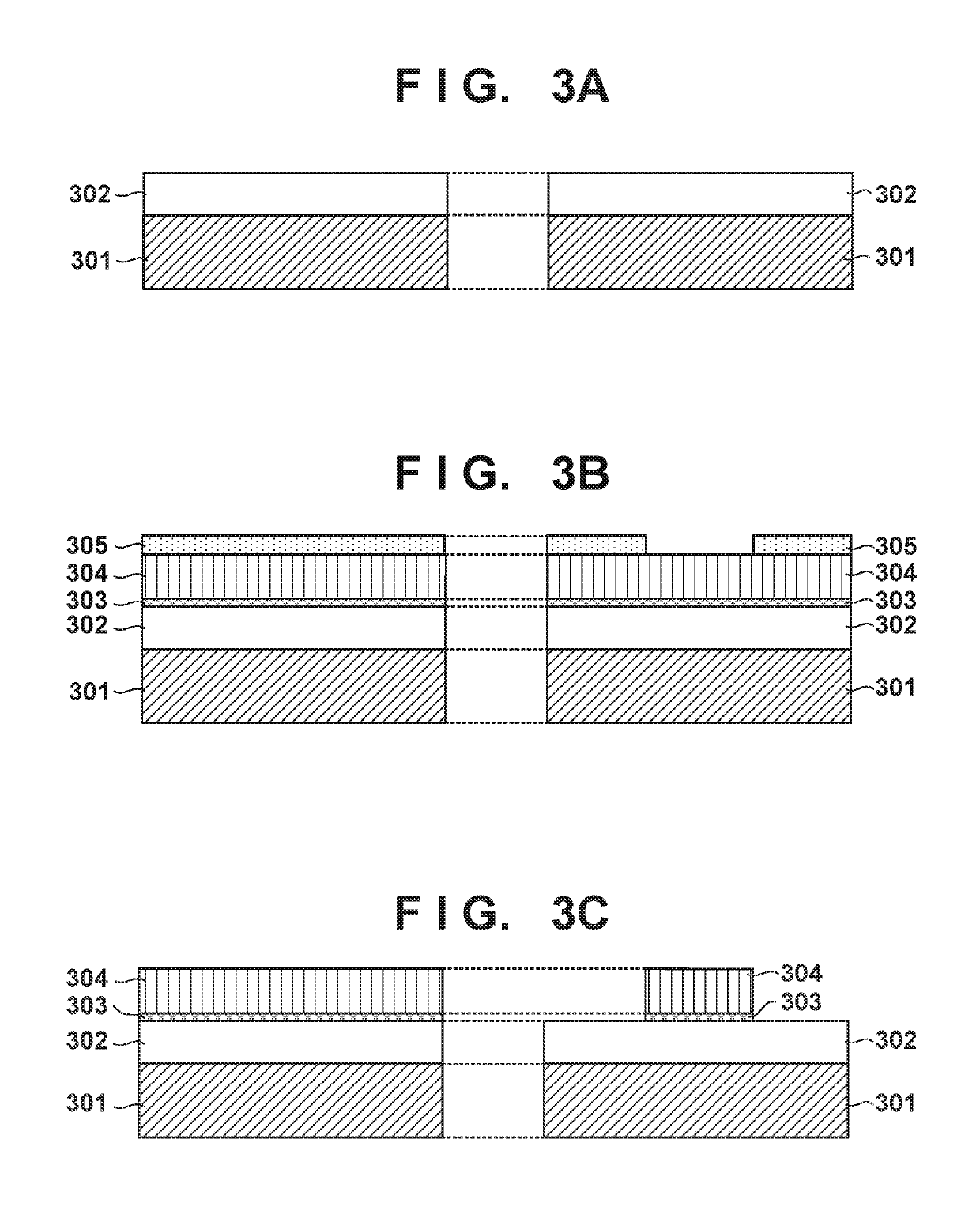
[0015...
second embodiment
[0037]A semiconductor device 400 according to the second embodiment will be described with reference to FIG. 4. A difference from the semiconductor device 100 of the first embodiment will mainly be described, and a description of an arrangement which may be the same will be omitted. The semiconductor device 400 includes a plurality of (two in this example) regions 109 in which a plurality of discharge heaters 101 are arranged. The semiconductor device 400 can discharge ink at a twofold density by including two columns of the plurality of discharge heaters 101.
[0038]These two regions 109 are arranged in a y-axis direction, and a liquid supply port 401 is located between them. The liquid supply port 401 is a through hole for supplying a liquid. A plurality of units 209 are arranged on a positive side in the y-axis direction with respect to the upper region 109. The plurality of units 209 are arranged on a negative side in the y-axis direction with respect to the lower region 109. By t...
third embodiment
[0039]A semiconductor device 500 according to the third embodiment will be described with reference to FIG. 5. A difference from the semiconductor device 100 of the first embodiment will mainly be described, and a description of an arrangement which may be the same will be omitted. The semiconductor device 500 includes a plurality of (six in this example) regions 109 in which a plurality of discharge heaters 101 are arranged. Liquid supply ports 401 are arranged between the regions 109 of the first column and the second column from the top, between the regions 109 of the third column and the fourth column, and between the regions 109 of the fifth column and the sixth column. Liquids different in color may be supplied to these three liquid supply ports 401, and the discharge heater 101 of each column may have a shape corresponding to a color.
[0040]A plurality of units 209 arranged in an x-axis direction are arranged on a positive side of the region 109 of the first column in a y-axis...
PUM
| Property | Measurement | Unit |
|---|---|---|
| angle | aaaaa | aaaaa |
| angle | aaaaa | aaaaa |
| angle | aaaaa | aaaaa |
Abstract
Description
Claims
Application Information
 - R&D
- Intellectual Property
- Life Sciences
- Materials
- Tech Scout
- Unparalleled Data Quality
- Higher Quality Content
- 60% Fewer Hallucinations
Browse by: Latest US Patents, China's latest patents, Technical Efficacy Thesaurus, Application Domain, Technology Topic, Popular Technical Reports.
© 2025 PatSnap. All rights reserved.Legal|Privacy policy|Modern Slavery Act Transparency Statement|Sitemap|About US| Contact US: help@patsnap.com