
Array substrate and manufacturing method thereof and display device

a manufacturing method and array substrate technology, applied in the field of array substrate and manufacturing method thereof, can solve problems such as deterioration of components' properties, and achieve the effects of preventing thermal problems, enhancing heat dissipation efficiency, and ensuring dissipation

Active Publication Date: 2019-11-19
SHENZHEN CHINA STAR OPTOELECTRONICS SEMICON DISPLAY TECH CO LTD
View PDF6 Cites 0 Cited by
  • Summary
  • Abstract
  • Description
  • Claims
  • Application Information

AI Technical Summary

Benefits of technology

The solution effectively reduces thermal issues, improves drive device performance, and prevents metal wire disconnection by uniformly dissipating heat, thereby enhancing the array substrate's heat dissipation efficiency and product yield.

Problems solved by technology

However, such metal wirings and the TFTs generate joule heating when electrical currents flow therethrough, and thus, temperatures of components in the array substrate increase, leading to deterioration of the properties of the components.
Particularly, the heating issues are even more seriously at sites where the metal wirings are connected with vias and this may cause burn-out of the vias, and eventually leads to disconnection.

Method used


Image

  • Array substrate and manufacturing method thereof and display device
  • Array substrate and manufacturing method thereof and display device
  • Array substrate and manufacturing method thereof and display device

Examples


first embodiment

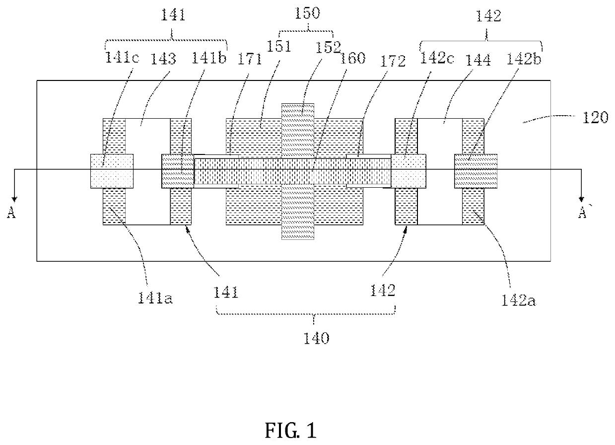
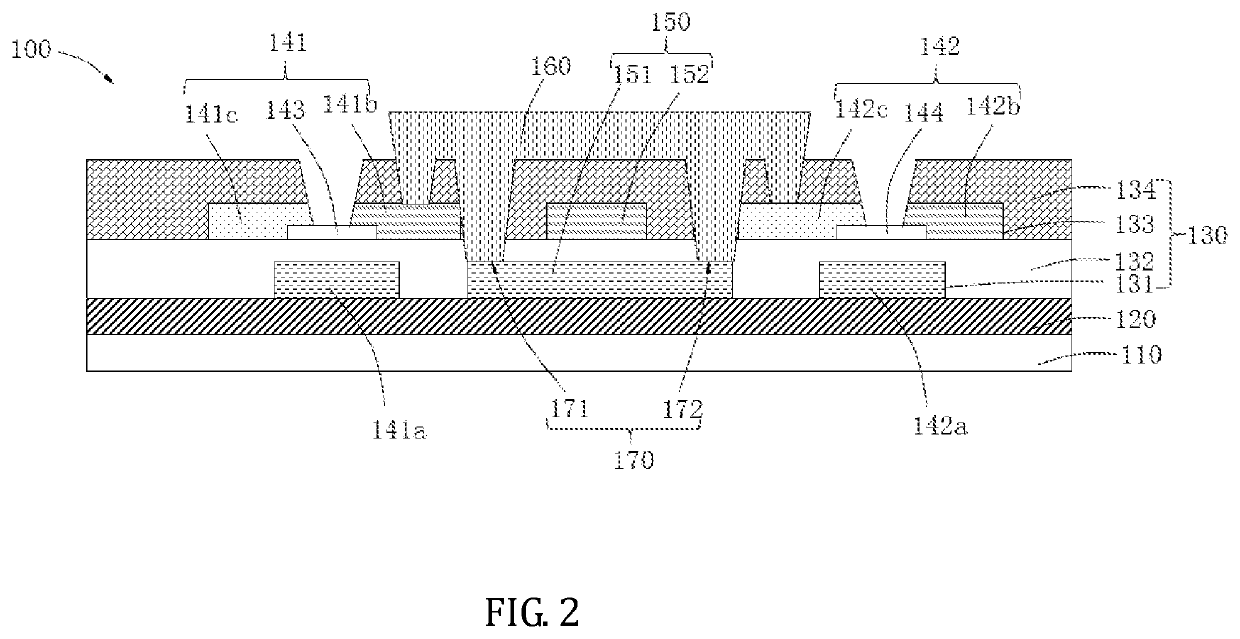
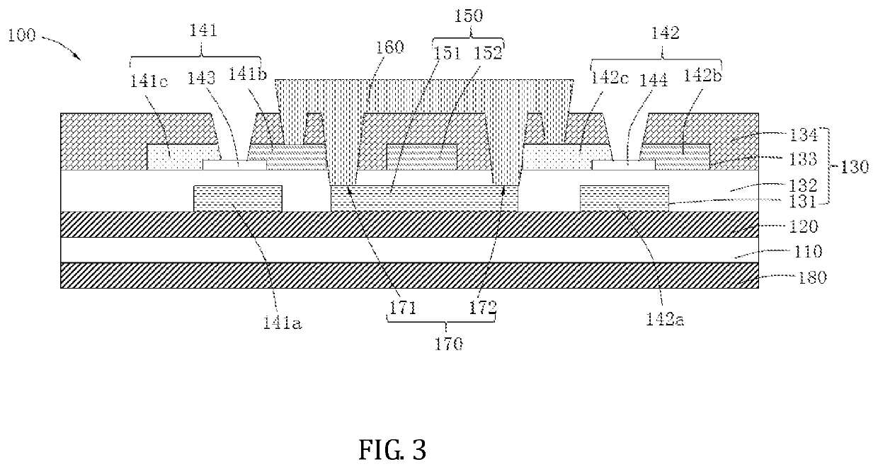
[0033]Referring to FIGS. 1 and 2, FIG. 1 shows an array substrate provided in this application. FIG. 2 is a cross-sectional view taken in direction AK of FIG. 1. The array substrate 100 comprises a carrier plate 110, a first heat dissipation layer 120, and a function layer 130 that are arranged to stack, in sequence, on each other, wherein the function layer 130 is arranged on one side that faces a user. The function layer 130 comprises a plurality of drive devices 140 and metal wires 150 and connection sections 160 arranged between the plurality of drive devices 140. The plurality of drive devices 140 are provided therein with openings 170, and the connection sections 160 are each arranged to connect, at one end thereof, with one of the drive devices 140 by way of the openings 170 and to connect an adjacent one of the drive devices 140 with an opposite end thereof that extend across and over the metal wires 150. The first heat dissipation layer 120 conducts heat generated by the me...

third embodiment

[0041]Referring to FIGS. 4 and 5, FIG. 4 shows an array substrate 100 provided in this application. FIG. 5 is a cross-sectional view taken in direction BB′ of FIG. 4. The function layer 130 comprises drive device zones 145, a metal wire zone 153, and a connection section zone 161. The drive device zones 145 comprise drive devices 140 arranged therein; the metal wire zone 153 comprises a metal wire 150 arranged therein; and the connection section zone 161 comprises a connection section 160 arranged therein. The first heat dissipation layer 120 has an orthogonal project on the function layer 130 that fall within the metal wire zone 153, the drive device zone 145 and the connection section zone 161. Such an arrangement is made for patterning of the first heat dissipation layer 120a and such as first heat dissipation layer 120a is located under the metal wire 150, the connection section 160, and the drive devices 140 so as to prevent interference with signal transmission made in other c...


PUM


Abstract

An array substrate includes a carrier plate, a first heat dissipation layer, and a function layer sequentially stacked on each other. The function layer is arranged on one side facing a user. The function layer includes a plurality of drive devices, metal wires and connection sections arranged between the plurality of drive devices. The plurality of drive devices are formed with openings. The connection sections each have an end extending through the openings to connect with one of the drive devices and an opposite end extending across the metal wires to connect with an adjacent one of the drive devices. The first heat dissipation layer conducts heat from the metal wires, the plurality of drive devices, and the connection sections through the carrier plate for dissipation. A method for manufacturing the array substrate and a display device are also provided.

Description

CROSS REFERENCE TO RELATED APPLICATIONS[0001]This application claims the priority of Chinese Patent Application No. 201710488943.7 filed on Jun. 23, 2017, titled “Array Substrate and Manufacturing Method Thereof and Display Device”, the disclosure of which is incorporated herein by reference in its entirety.BACKGROUND OF THE INVENTION1. Field of the Invention[0002]The present invention relates to the field of electronic equipment, and more particularly to an array substrate and a manufacturing method thereof, and a display device.2. The Related Arts[0003]With the consumers' increasing demands for finer and finer resolution of display devices and increasing expansion of sizes of the display devices, as well as exacted pursuit for visual effects achievable with ultra slim bezels, metal wirings of the display devices are subjected to increasingly denser arrangements. For example, to have an increased resolution of a display device, an increased number of thin-film transistors (TFTs) mu...

Claims


Application Information

Patent Timeline
Patent Type & Authority Patents(United States)
IPC IPC(8): H01L27/12H01L23/36H01L23/34
CPCH01L27/1285H01L27/1214H01L27/124H01L23/36H01L23/34H01L23/367G02F1/133385G02F2201/36H01L27/1251H01L27/1218G02F1/136295H10K59/8794H10K59/00
Inventor LI, WENYINGLIU, XIAODI
Owner SHENZHEN CHINA STAR OPTOELECTRONICS SEMICON DISPLAY TECH CO LTD
Learn More