Electronic circuit package having high composite shielding effect
a composite shielding and electronic circuit technology, applied in shielding materials, semiconductor devices, semiconductor/solid-state device details, etc., can solve problems such as difficult to achieve height reduction, difficult to solve malfunction and radio disturbance, and difficult to connect metal films to power supply patterns. , to achieve the effect of reducing the risk of electromagnetic interferen
- Summary
- Abstract
- Description
- Claims
- Application Information
AI Technical Summary
Benefits of technology
Problems solved by technology
Method used
Image
Examples
first embodiment
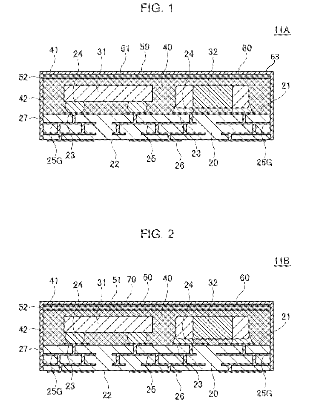
[0035]FIG. 1 is a cross-sectional view illustrating a configuration of an electronic circuit package 11A according to the first embodiment of the present invention.
[0036]As illustrated in FIG. 1, the electronic circuit package 11A according to the present embodiment includes a substrate 20, a plurality of electronic components 31 and 32 mounted on the substrate 20, a magnetic mold resin 40 covering a front surface 21 of the substrate 20 so as to embed the electronic components 31 and 32, a magnetic film 50 covering the magnetic mold resin 40, and a metal film 60 covering the magnetic film 50 and the magnetic mold resin 40.
[0037]Although the type of the electronic circuit package 11A according to the present embodiment is not especially limited, examples thereof include a high-frequency module handling a high-frequency signal, a power supply module performing power supply control, an SIP (System-In-Package) having a 2.5D structure or a 3D structure, and a semiconductor package for ra...
second embodiment
[0075]FIG. 8 is a cross-sectional view illustrating a configuration of an electronic circuit package 12A according to the second embodiment of the present invention.
[0076]As illustrated in FIG. 8, the electronic circuit package 12A according to the present embodiment differs from the electronic circuit package 11A of FIG. 1 according to the first embodiment in that the magnetic film 50 covers not only the top surface 41 of the magnetic mold resin 40, but also the side surface 42. Other configurations are the same as those of the electronic circuit package 11A according to the first embodiment. Thus, in FIG. 8, the same reference numerals are given to the same elements as in FIG. 1, and repeated descriptions will be omitted.
[0077]In the present embodiment, the side surface 42 of the magnetic mold resin 40 is fully covered with the magnetic film 50, and thus, a part where the magnetic mold resin 40 and metal film 60 contact each other does not substantially exist. With this configurat...
third embodiment
[0085]FIG. 14 is a cross-sectional view illustrating a configuration of an electronic circuit package 13A according to a third embodiment of the present invention.
[0086]As illustrated in FIG. 14, the electronic circuit package 13A according to the present embodiment differs from the electronic circuit package 11A illustrated in FIG. 1 in that the magnetic film 50 is formed on an upper surface 61 of the metal film 60. That is, the positional relationship between the magnetic film 50 and the metal film 60 constituting the laminated film is reversed. Other configurations are the same as those of the electronic circuit package 11A illustrated in FIG. 1. Even with this configuration, high composite shielding effect can be achieved since a triple-shield structure composed of the magnetic mold resin 40, magnetic film 50, and metal film 60 can be obtained.
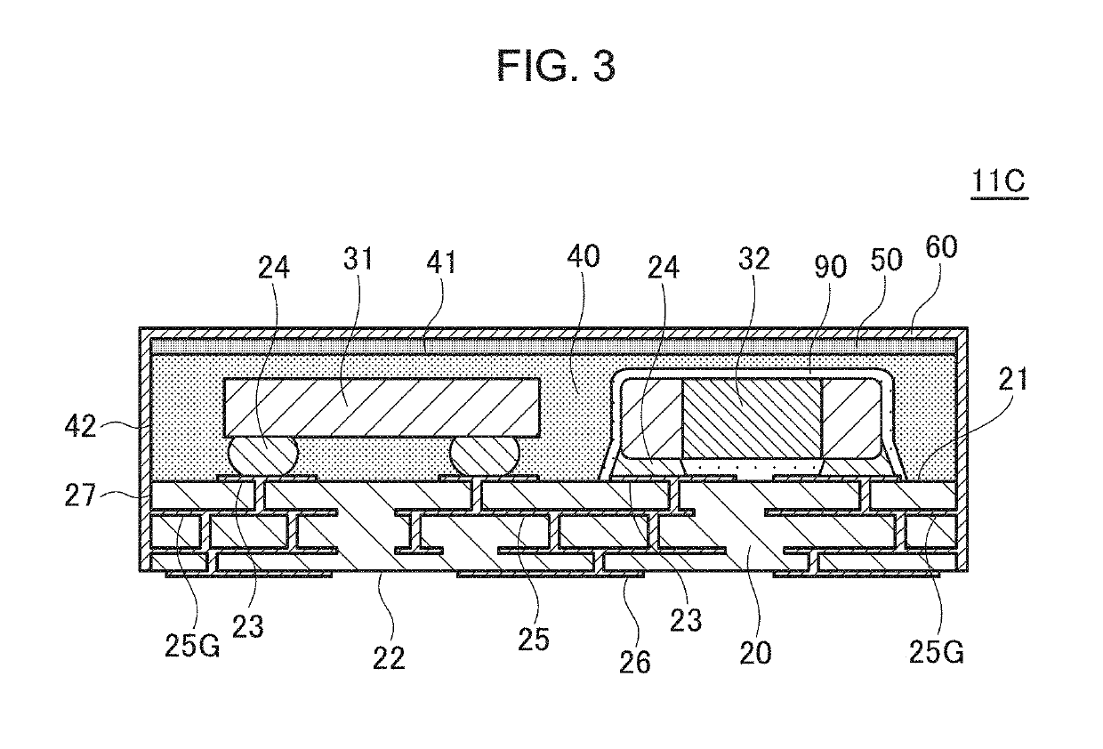
[0087]When it is difficult to directly form the magnetic film 50 on the upper surface 61 of the metal film 60, a thin adhesive layer 70 c...
PUM
 Abstract
Description
Claims
Application Information
 - R&D
- Intellectual Property
- Life Sciences
- Materials
- Tech Scout
- Unparalleled Data Quality
- Higher Quality Content
- 60% Fewer Hallucinations
Browse by: Latest US Patents, China's latest patents, Technical Efficacy Thesaurus, Application Domain, Technology Topic, Popular Technical Reports.
© 2025 PatSnap. All rights reserved.Legal|Privacy policy|Modern Slavery Act Transparency Statement|Sitemap|About US| Contact US: help@patsnap.com


