Semiconductor device and method of forming the same

a technology of semiconductors and semiconductors, applied in the direction of semiconductor devices, electrical devices, transistors, etc., can solve the problems of current leakage and poor electrical performan

Active Publication Date: 2019-02-26
UNITED MICROELECTRONICS CORP
View PDF3 Cites 1 Cited by
  • Summary
  • Abstract
  • Description
  • Claims
  • Application Information

AI Technical Summary

Benefits of technology

[0004]It is one of the primary objectives of the present invention to provide a semiconductor device and a method of forming the same, in which, different isolation structures are formed respectively on two fin shaped structures, so as to improve the isolation function and to provide corresponding stress thereto. In this way, it is sufficient to obtain a more reliable semiconductor device.
[0008]The two isolation structures may isolate the two fin shaped structures, and further provide suitable stresses to the channel regions of a PFET / NFET device which is formed subsequently on the two fin shaped structures. The isolation structure disposed in the PFET device preferably includes a monolayer structure, and which is disposed directly on the top surface of the fin shaped structure. On the other hand, the isolation structure disposed in the NFET device preferably includes a multilayer structure, and which is partially disposed within the fin shaped structure, with the top surface thereof being lower than the top surface of the fin shaped structure.

Problems solved by technology

However, under the requirements of continuous miniaturization, the designs and fabricating processes of current FinFET structure still face more challenges and limitations, leading to current leakage and poor electrical performance thereby.

Method used


Image

  • Semiconductor device and method of forming the same
  • Semiconductor device and method of forming the same
  • Semiconductor device and method of forming the same

Examples


first embodiment

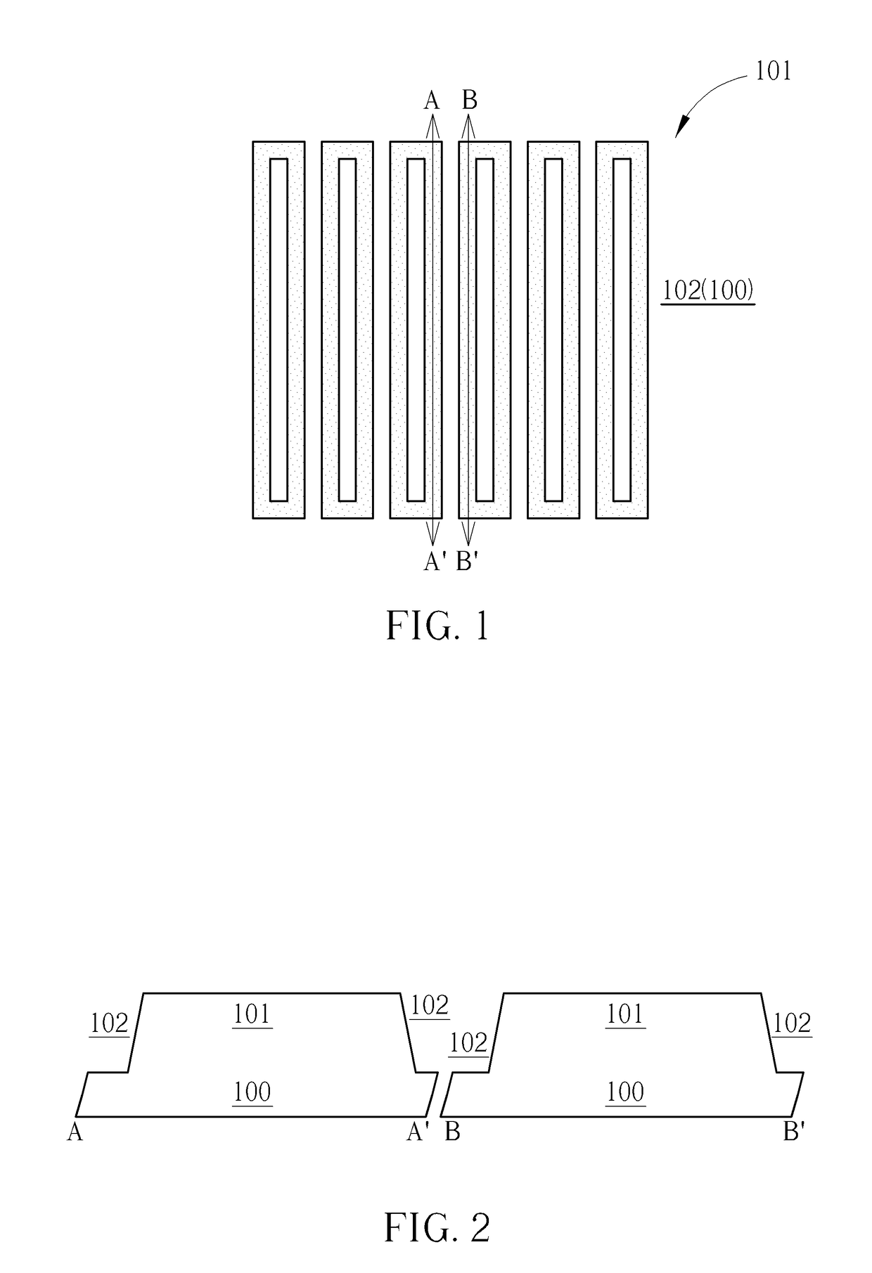
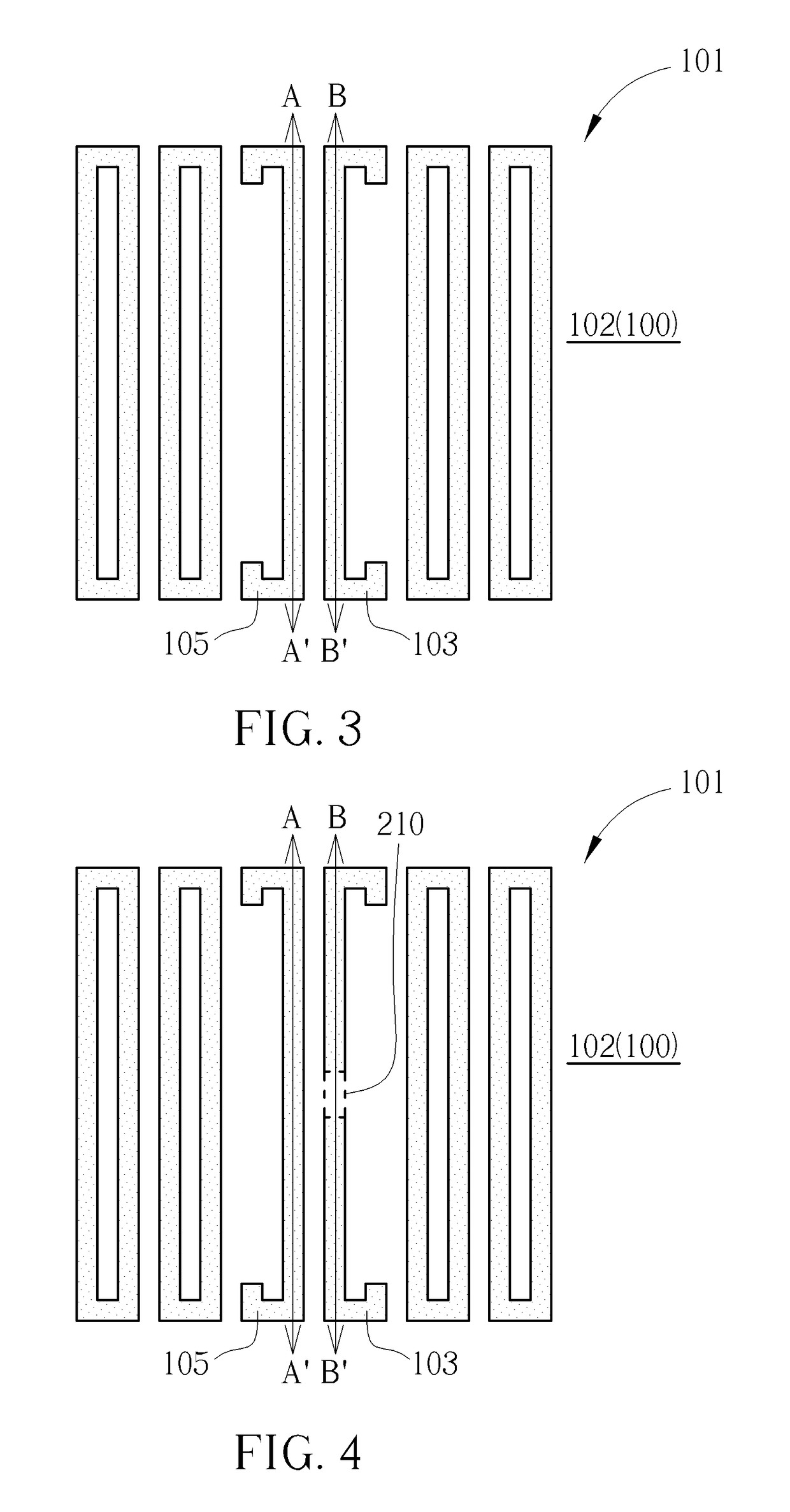
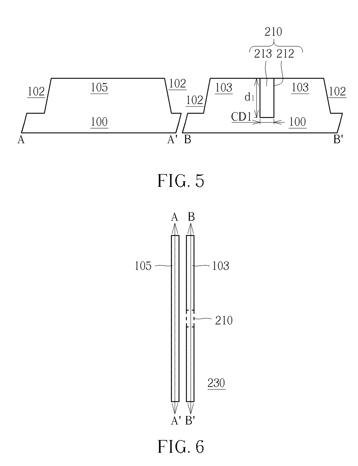
[0027]Please refer to FIG. 1 to FIG. 10, which are schematic diagrams illustrating a method of forming a semiconductor device according to the present invention, wherein FIGS. 1, 3, 4, 6 and 8 show top views of the semiconductor device in forming steps, and others drawings show cross-sectional views taken along the cross lines A-A, B-B′ in forming steps.

[0028]First of all, a substrate 100 is provided, and the substrate 100 for example includes a silicon substrate, a silicon-containing substrate or a silicon-on-insulator (SOI) substrate. A plurality of fins 101 are formed on a surface of the substrate 100, with each of the fins 101 having a closed rectangular frame, parallel extended along a same direction (not shown in the drawings, such as a y-direction), as shown FIG. 1. In one embodiment, the formation of the fins 101 is for example accomplished through a sidewall image transfer (SIT) technique. The SIT technique may include performing a lithography and etching process on a bulk ...

second embodiment

[0046]According to the above processes, the method of forming a semiconductor device of the present invention is accomplished. Besides disposing the isolation structures 210, 250 with different materials, different heights and structures in two different fin shaped structures 103, 105, a monolayered isolation structure 210a, or a multilayered isolation structure 250a may be additionally disposed between the two fin shaped structures 103, 105, to further isolate the two fin shaped structures 103, 105. In this way, those disposed isolation structures either within or between the fin shaped structures 103, 105 may provide better functions to improve the current leakage issues and electrical performance of the entire device, and a more reliable semiconductor device can be obtained in the present invention.

[0047]Overall speaking, through the method of the present invention, two isolation structures with different materials, different heights and different structures are respectively form...


PUM


Abstract

A semiconductor device and a method of forming the same, the semiconductor device includes a first and a second fin structures, a first, a second and a third isolation structures, and a first and a second gate structures. The first and second fin structures are disposed in a substrate. The first isolation structure is disposed in the substrate and surrounds the first and second fin structures. The second isolation structure is disposed in the first fin structure, and a top surface of the second isolation structure is leveled with a top surface of the first and second fin structures. The third isolation structure is disposed in the second fin shaped structure, and a top surface of the third isolation structure is lower than the top surface of the first and second fin structures. The first and second gate structures are disposed on the second and third isolation structures, respectively.

Description

BACKGROUND OF THE INVENTION1. Field of the Invention[0001]The present invention relates to a semiconductor device and a method of forming the same, and more particularly, to a semiconductor device having multiple isolation structure and a method of forming the same.2. Description of the Prior Art[0002]With the trend in the industry being towards scaling down the size of the metal oxide semiconductor transistors (MOS), three-dimensional or non-planar transistor technology, such as fin field effect transistor technology (FinFET) has been developed to replace planar MOS transistors. Since the three-dimensional structure of a FinFET increases the overlapping area between the gate and the fin-shaped structure of the silicon substrate, the channel region can therefore be more effectively controlled. This way, the drain-induced barrier lowering (DIBL) effect and the short channel effect are reduced. The channel region is also longer for an equivalent gate length, thus the current between t...

Claims


Application Information

Patent Timeline
Patent Type & Authority Patents(United States)
IPC IPC(8): H01L29/78H01L21/8238H01L27/092H01L29/06H01L21/82
CPCH01L29/7846H01L21/823821H01L29/0653H01L27/0924H01L21/823878
Inventor CHENG, CHI-HSUANCHIU, CHENG-PUSU, YU-CHIHWANG, CHIH-YIHSIEH, CHIN-YANGHSU, TIEN-SHANWANG, YAO-JHAN
Owner UNITED MICROELECTRONICS CORP
Why Eureka
Try Eureka