Electro-optical device and electronic apparatus having an evaluation pattern
a technology of electronic apparatus and optical device, which is applied in the direction of static indicating device, optical element, instruments, etc., can solve the problems of difficult to accurately measure the dimension and position of each of the coloring layers, and achieve the effect of excellent display quality
- Summary
- Abstract
- Description
- Claims
- Application Information
AI Technical Summary
Benefits of technology
Problems solved by technology
Method used
Image

Examples
first embodiment
Organic EL Device
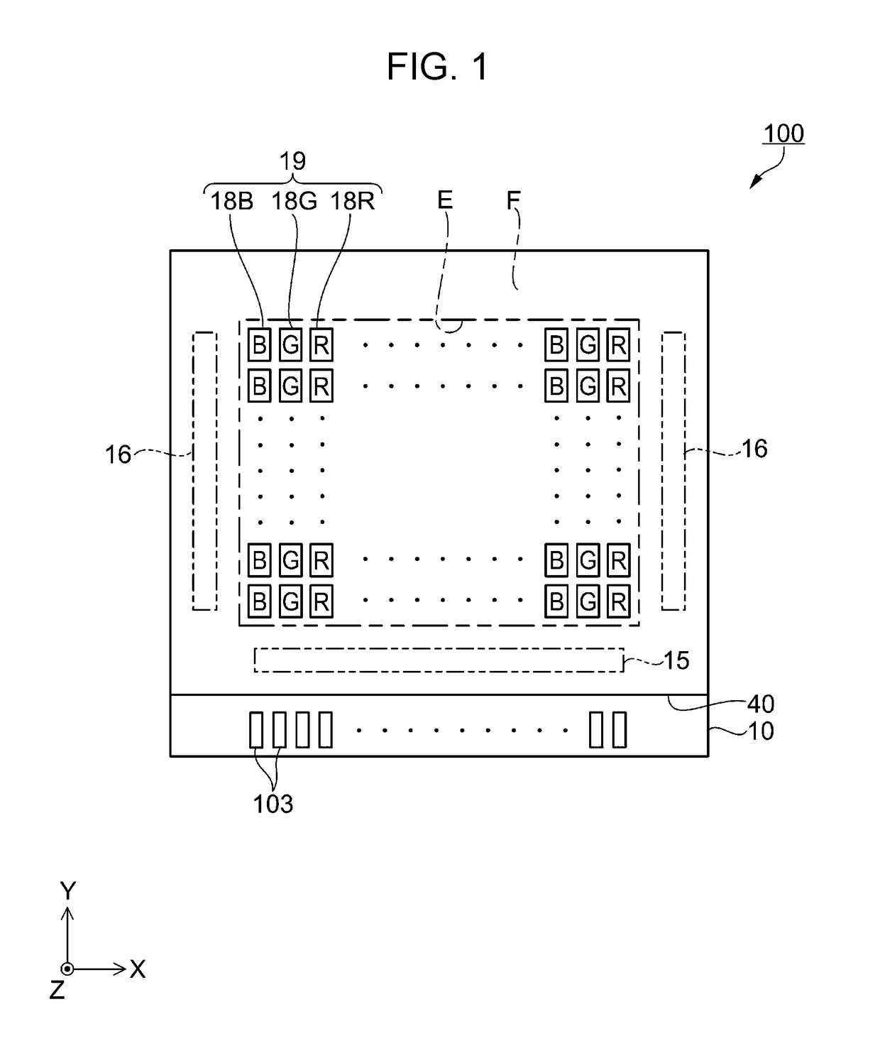
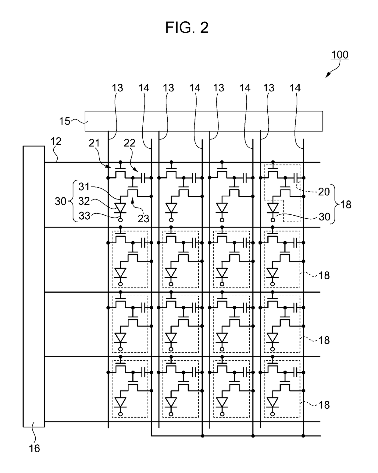
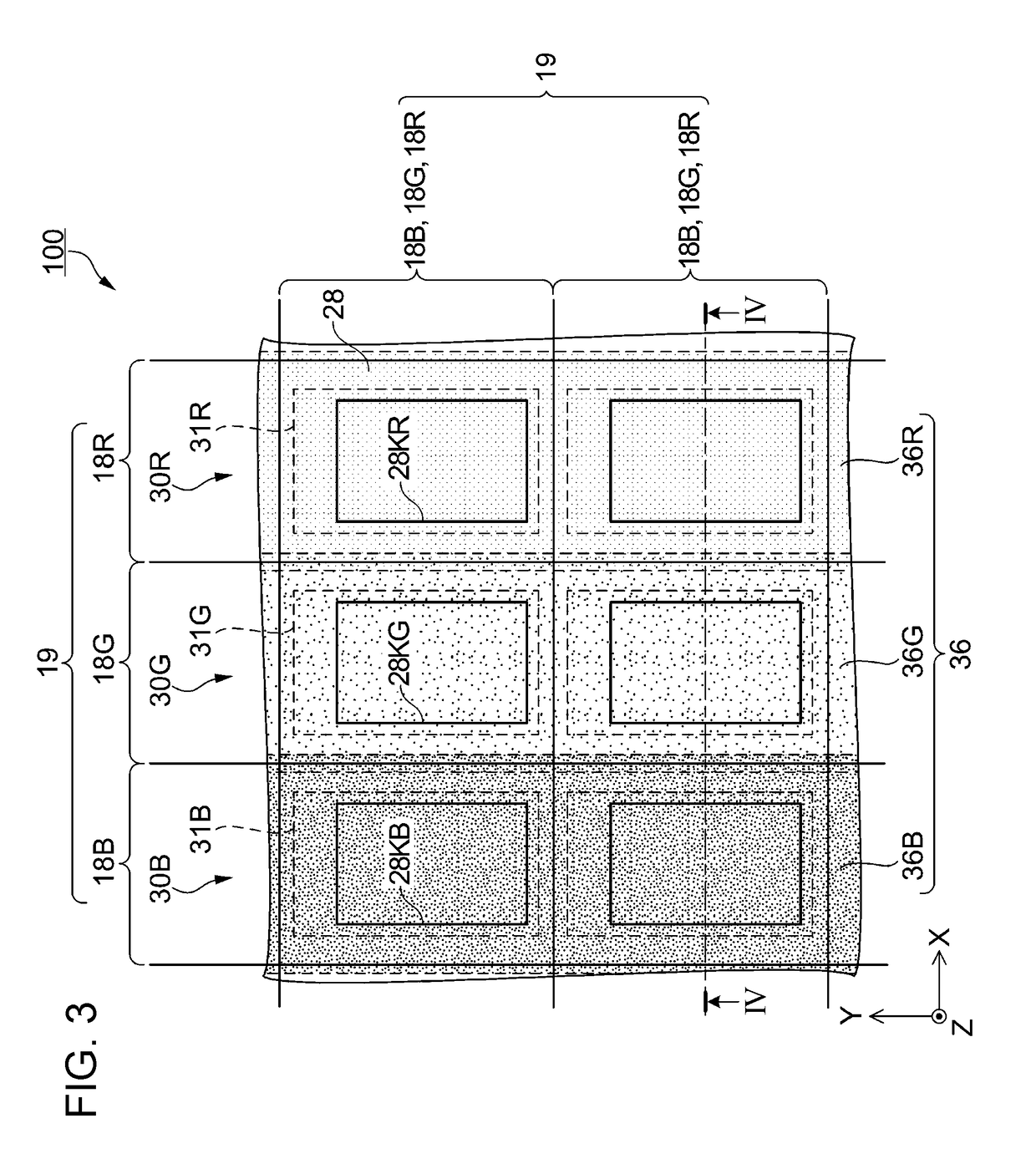
[0049]First, an organic EL device as an electro-optical device according to a first embodiment will be described with reference to FIG. 1 to FIG. 4. FIG. 1 is a schematic plan view illustrating a configuration of the organic EL device according to the first embodiment. FIG. 2 is an equivalent circuit diagram illustrating an electrical configuration of the organic EL device according to the first embodiment. FIG. 3 is a schematic plan view illustrating disposition of the organic EL element and a color filter in a sub pixel. FIG. 4 is a schematic cross-sectional view illustrating a configuration of the sub pixel taken along line IV-IV in FIG. 3. An organic EL device 100 according to the present embodiment is a self-luminous type microdisplay appropriate to a display unit of a head mount display (HMD) to be described below.
[0050]As shown in FIG. 1, the organic EL device 100 according to the preset embodiment includes an element substrate 10 and a protective substrate 4...
example 1
[0108]First, Example 1 of the evaluation pattern according to the present embodiment will be described with reference to FIG. 5A, FIG. 5B, and FIG. 6. FIG. 5A is a schematic plan view of an element substrate showing disposition of a dimension evaluation pattern according to Example 1. FIG. 5B is a schematic plan view illustrating the enlarged dimension evaluation pattern. FIG. 6 is a schematic cross-sectional view illustrating disposition of the dimension evaluation pattern taken along line VI-VI in FIG. 5A. FIG. 14 is a schematic cross-sectional view of the element substrate illustrating disposition of a dimension evaluation pattern according to a comparative example.
[0109]FIG. 5A is a diagram when the element substrate 10 on which the layers up to the color filter 36 (see FIG. 4) are formed is seen in a plan view. As shown in FIG. 5A, a color filter light shielding unit (hereinafter, referred to as CF light shielding unit) 36S is disposed in the non-display area F of the element s...
example 2
[0132]Subsequently, Example 2 of the evaluation pattern according to the present embodiment will be described with reference to FIG. 7 and FIG. 8. FIG. 7 is a schematic plan view of an element substrate showing disposition of an evaluation pattern according to Example 2. FIG. 8 is a schematic cross-sectional view illustrating disposition of the evaluation pattern taken along line VIII-VIII in FIG. 7. Here, differences with respect to Example 1 will be only described.
[0133]As shown in FIG. 7, in Example 2, the dimension evaluation pattern 50 is disposed at a substantially central portion in the longitudinal direction (X direction) of one side of the −Y direction side of the CF light shielding unit 36S and near the display area E in a width direction (Y direction). As shown FIG. 8, also in Example 2, the dimension evaluation pattern 50 is disposed on the sealing part 34 including the three layers of the first sealing layer 34a, the planarization layer 34b, and the second sealing layer...
PUM
 Abstract
Description
Claims
Application Information
 - R&D
- Intellectual Property
- Life Sciences
- Materials
- Tech Scout
- Unparalleled Data Quality
- Higher Quality Content
- 60% Fewer Hallucinations
Browse by: Latest US Patents, China's latest patents, Technical Efficacy Thesaurus, Application Domain, Technology Topic, Popular Technical Reports.
© 2025 PatSnap. All rights reserved.Legal|Privacy policy|Modern Slavery Act Transparency Statement|Sitemap|About US| Contact US: help@patsnap.com