
Semiconductor memory device

一种存储装置、半导体的技术,应用在半导体器件、信息存储、静态存储器等方向,能够解决控制器控制复杂、电气功耗限制、控制复杂等问题,达到增强电流提供能力、增加有效栅极宽度、提高写操作速度的效果

Active Publication Date: 2007-05-30
MICRON TECH INC
View PDF2 Cites 7 Cited by
  • Summary
  • Abstract
  • Description
  • Claims
  • Application Information

AI Technical Summary

Problems solved by technology

This makes DRAM unsuitable for storage of program and archive information
In addition, even when the power is turned on, the device must periodically perform a refresh operation to maintain the stored data, so there is a limit to the amount of device electrical power consumption that can be reduced, and there is also a problem that the control performed by the controller is very complicated
However, when such a transistor is provided, for example, the bit line needs to be temporarily suspended, so the control becomes complicated

Method used


Image

  • Semiconductor memory device
  • Semiconductor memory device
  • Semiconductor memory device

Examples


Embodiment Construction

[0059] Hereinafter, preferred embodiments of the present invention will be explained in detail with reference to the accompanying drawings.

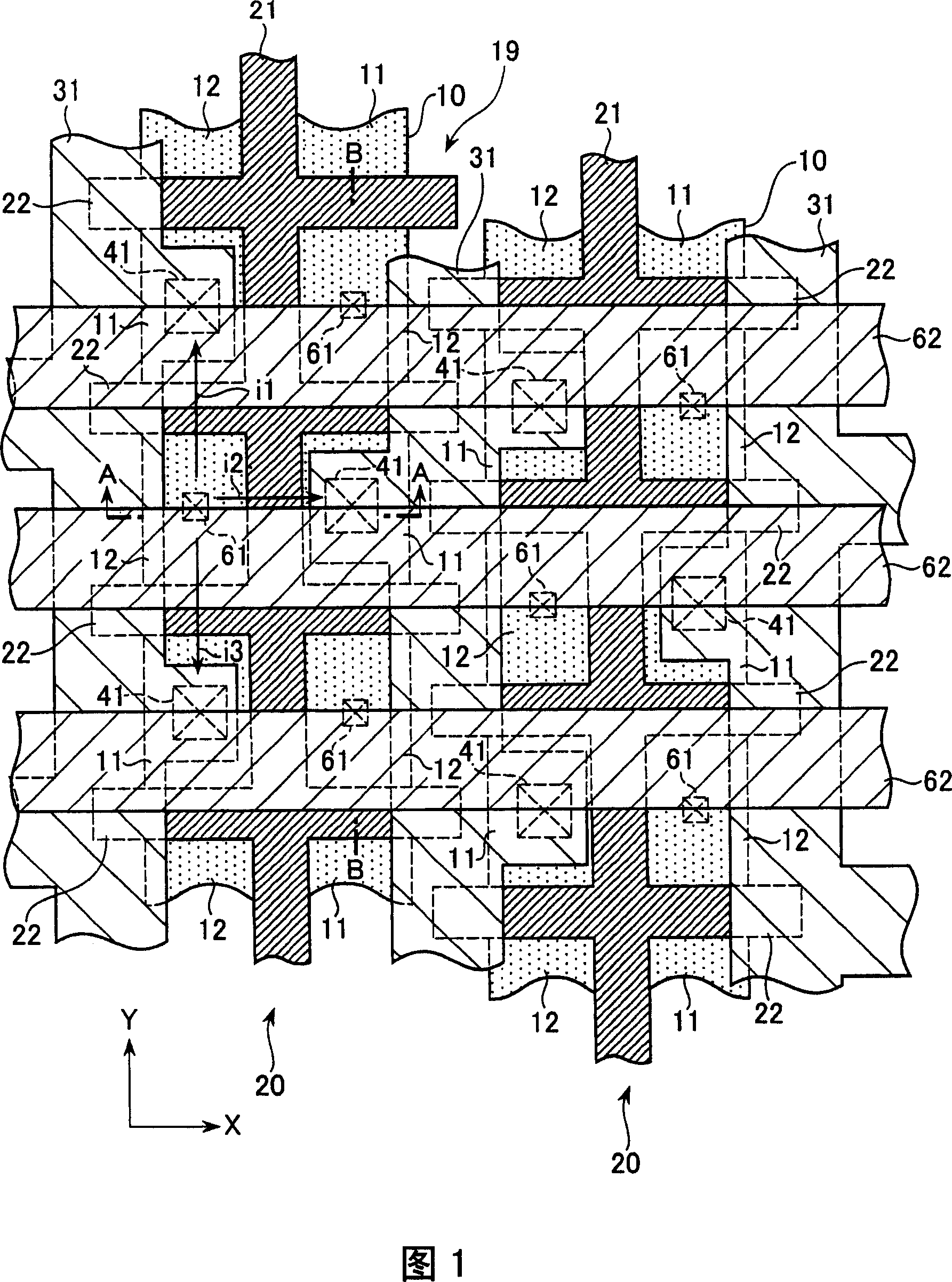
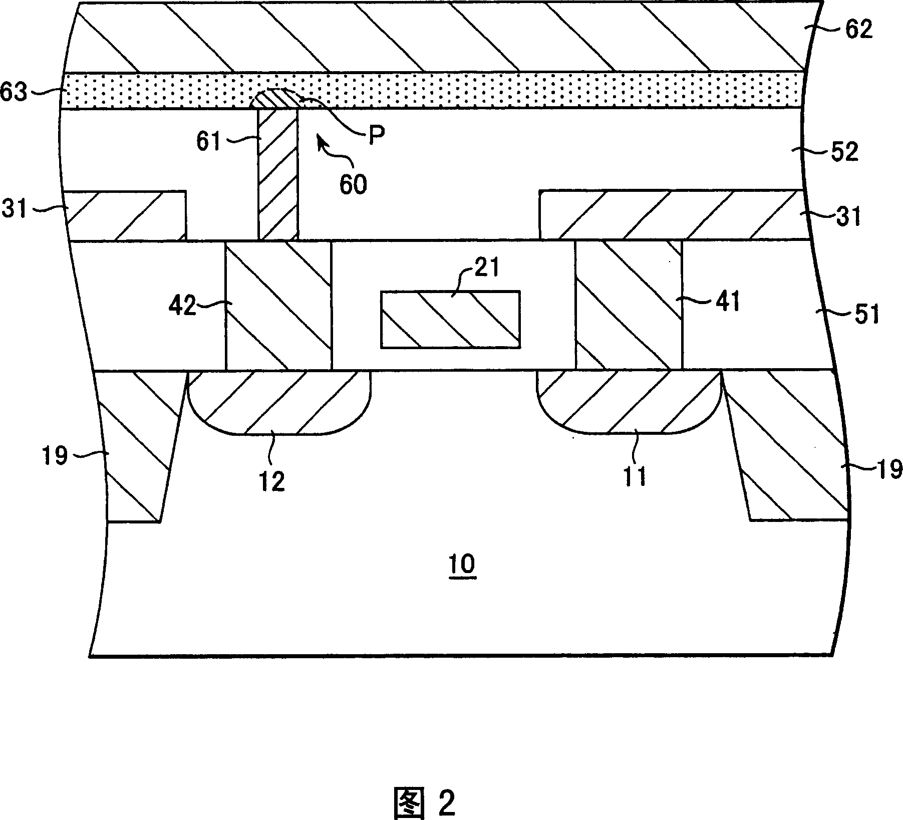
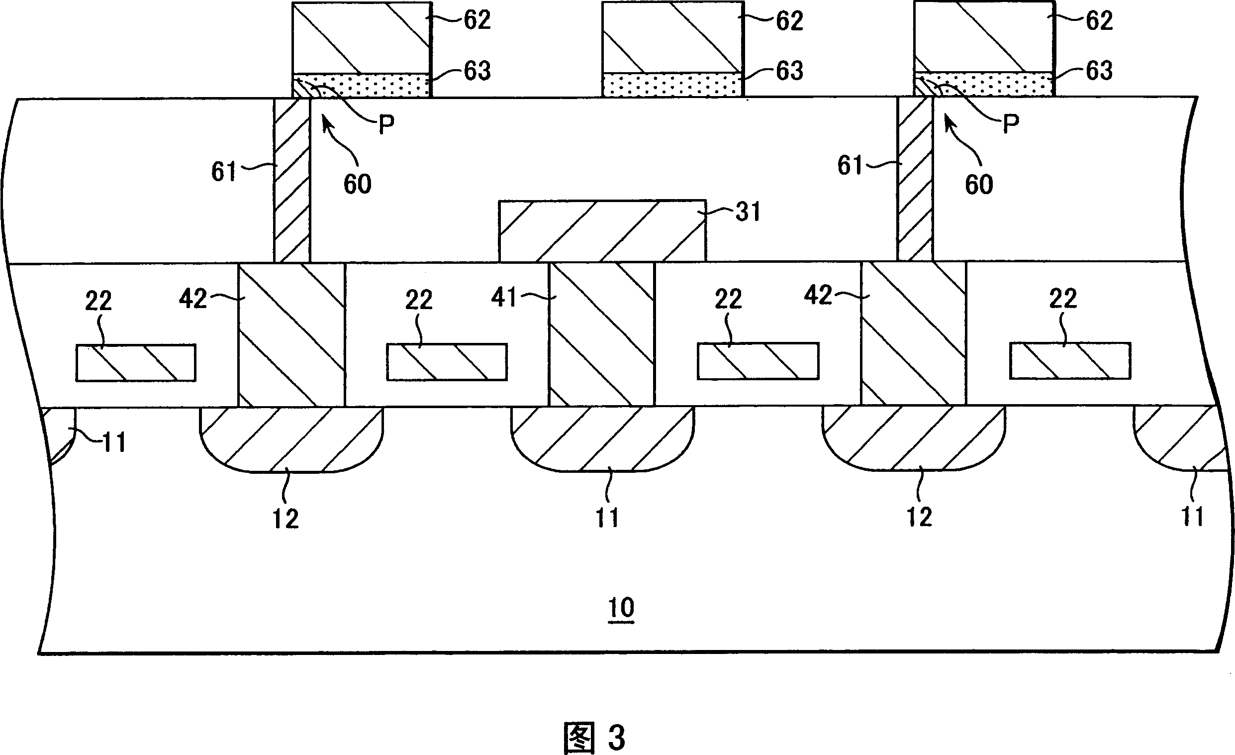
[0060] FIG. 1 is a schematic plan view of a relevant portion of a semiconductor memory device according to a preferred embodiment of the present invention. Fig. 2 is a schematic cross-section along line A-A in Fig. 1 . Fig. 3 is a schematic cross-section along line B-B in Fig. 1 . This embodiment is the preferred embodiment when the present invention is applied to PRAM

[0061] Example.

[0062] As shown in FIG. 1 , the semiconductor memory device according to the present embodiment includes a plurality of active regions 10 , and a gate electrode 20 arranged in a fishbone shape on each active region 10 .

[0063] The active region 10 extends along the Y direction shown in FIG. 1 . Between the active regions 10 along the X direction, element isolation regions 19 are adjacently arranged. In the active region 10, a plurality of source ...


PUM


Abstract

A semiconductor memory device includes a plurality of active regions, and a gate electrode in a fish bone shape arranged on each active region. In each active region, a plurality of source regions and a plurality of drain regions are arranged in a matrix manner. The source regions are commonly connected to a source line, and the drain regions are each connected to a lower electrode of a different memory element. According to the present invention, it is possible to assign three cell transistors connected in parallel to one memory element, so that an effective gate width is further increased.

Description

technical field [0001] The present invention relates to a semiconductor memory device. More specifically, the present invention relates to a semiconductor memory device that holds information according to the presence or absence of current flowing through a cell transistor, the magnitude of current flowing through a cell transistor, and the like. Background technique [0002] Personal computers, servers, and the like use hierarchically structured storage devices. Lower-tier memories are inexpensive and offer high storage capacity, while memories higher up in the hierarchy offer high-speed operations. The bottom layer typically includes magnetic storage, such as hard disks and magnetic tape. In addition to being non-volatile, magnetic memory is an inexpensive way to store more information than solid-state devices such as semiconductor memory. However, compared to the sequential access operations of magnetic memory devices, semiconductor memories operate faster and are capa...

Claims


Application Information

Patent Timeline
Patent Type & Authority Applications(China)
IPC IPC(8): H01L27/24H01L27/105H01L29/423G11C11/56
CPCH01L45/143H01L45/06G11C2213/79H01L45/1233H01L45/148H01L27/2436H01L27/24H01L45/144G11C13/003G11C2213/74G11C13/0004H01L27/2463G11C11/5678H10B63/30H10B63/80H10N70/8825H10N70/884H10N70/231H10N70/8828H10N70/826
Inventor 佐藤誉中井洁
Owner MICRON TECH INC
Learn More