
Manufacturing apparatus and method of optical device

A technology for optical devices and manufacturing devices, which is applied to optical components, optics, projection devices, etc., and can solve problems such as complex algorithms

Active Publication Date: 2011-11-16
SAMSUNG ELECTRONICS CO LTD
View PDF0 Cites 0 Cited by
  • Summary
  • Abstract
  • Description
  • Claims
  • Application Information

AI Technical Summary

Problems solved by technology

[0005] Moreover, the existing algorithm for waveform analysis for arraying prisms is relatively complicated, so it takes more effort to make the optical path length consistent

Method used


Image

  • Manufacturing apparatus and method of optical device
  • Manufacturing apparatus and method of optical device
  • Manufacturing apparatus and method of optical device

Examples


Embodiment Construction

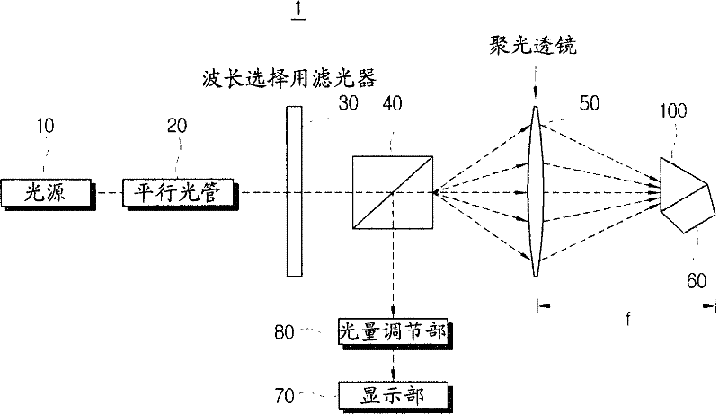
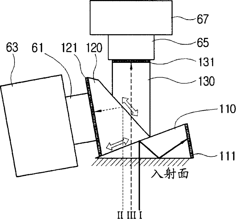
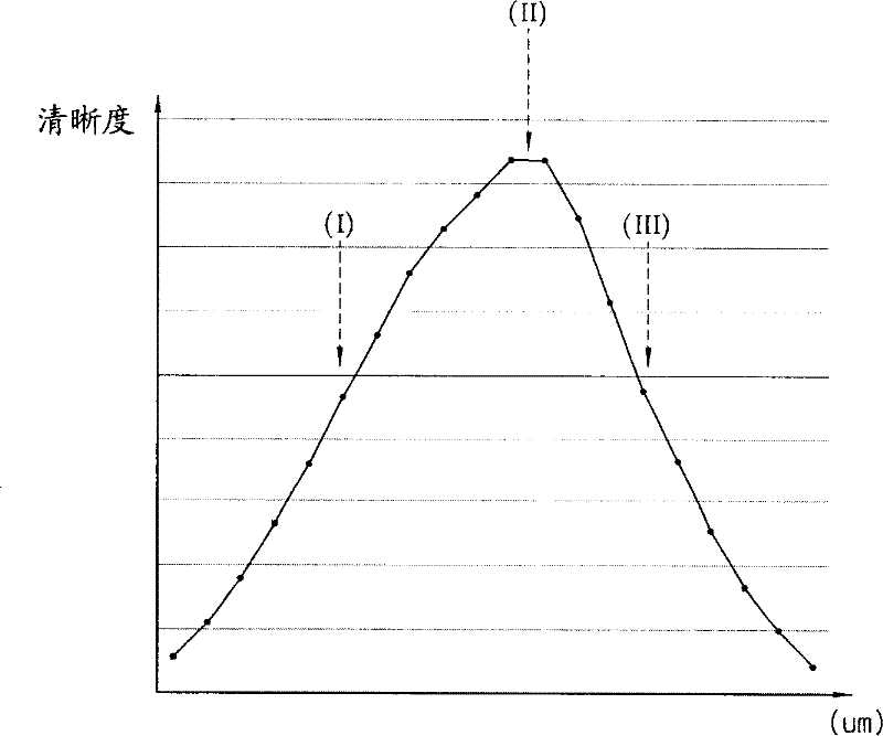
[0027] Hereinafter, embodiments of the present invention will be described in detail with reference to the drawings.

[0028] Refer below figure 1 Referring to FIG. 3 , an optical device manufacturing device provided by an embodiment of the present invention is illustrated.

[0029] figure 1 It is a schematic diagram of an optical device manufacturing device provided according to an embodiment of the present invention, figure 2 is a schematic diagram of the prism unit used to illustrate the long optical path length of the prism, Figure 3A and Figure 3B This is a schematic diagram illustrating the change in clarity of light corresponding to the movement of the prism.

[0030] An optical device manufacturing apparatus 1 includes a light source 10, a collimator 20, a wavelength selection filter 30, a light guide 40, a condenser lens 50, a holder 60 for adjusting the position of a prism, and a display for displaying reflected light. part 70 and light quantity adjusting p...


PUM


Abstract

The present invention provides a manufacturing apparatus of optical device which can easily make uniform of the length of optical path for plurality of prisms and manufacturing method thereof. The manufacturing apparatus of optical device with plurality of prisms provided according to the present invention, includes: a light source for emitting the light with predetermined pattern; a wavelength color selecting filter of the light that distilled from the emitted light with predetermined wavelength range; a focusing lens for focusing the light from the wavelength color selecting filter; a display part for displaying the pattern of the light reflected from the prism; a support for adjusting the position of the prism, making the definition of the pattern displayed on the display part in the predetermined range.

Description

technical field [0001] The present invention relates to a manufacturing device and a manufacturing method of an optical device, and more particularly to a manufacturing device and a manufacturing method of an optical device using a plurality of prisms. Background technique [0002] Charge-coupled devices (CCD: chargecoupled devices) used in optical devices for capturing and reproducing images have developed from 1-CCD to 3-CCD. For the conventional 1-CCD that can only display the brightness and shape of the input image, color filters are used on the CCD to reproduce the color. Although colors can be reproduced by using color filters, since one pixel can only contain information corresponding to one color in one RGB, there is a limitation in clearly expressing an image. [0003] Recently, in order to solve the above-mentioned problem and reproduce an image close to the real thing, a prism module including three specially coated prisms for performing RGB color decomposition a...

Claims


Application Information

Patent Timeline
Patent Type & Authority Patents(China)
IPC IPC(8): G02B27/00G02B7/18G03B21/00H04N23/16
CPCG02B7/343G02B27/1013G02B27/126G02B27/30G02B5/04
Inventor 李泰润闵炫轸赵成训普特波夫·维拉帝莫郑在贤李峻泳李锡原金重铉
Owner SAMSUNG ELECTRONICS CO LTD
Learn More