
NAND FLASH memory device

A storage device and data cache technology, applied in the field of non-volatile semiconductor storage devices, can solve problems such as writing information into bad blocks, and achieve the effects of simplifying communication, simple application, and widening the scope of application

Active Publication Date: 2007-03-28
SAGE MICROELECTRONICS CORP
View PDF0 Cites 10 Cited by
  • Summary
  • Abstract
  • Description
  • Claims
  • Application Information

AI Technical Summary

Problems solved by technology

[0005] (2) NAND FLASH cannot guarantee 100% good blocks (Block). Usually, NAND FLASH has 2% bad blocks, and these bad blocks are randomly distributed, so there must be a certain mechanism to manage these good blocks or bad blocks. Therefore, writing information to NAND FLASH requires considerable skills, because designers must not write information into bad blocks, which means that virtual mapping must be performed on NAND FLASH from beginning to end
[0007] At present, some external application-level CPUs cannot directly process these management algorithms of NAND FLASH, such as mobile phone baseband chips, especially ECC, which requires hardware implementation to ensure speed.
Therefore, at present, NOR FLASH is used to store programs and data in mobile phones, and NAND FLASH cannot be directly used as program and data storage for mobile phones.

Method used


Image

  • NAND FLASH memory device
  • NAND FLASH memory device
  • NAND FLASH memory device

Examples


Embodiment Construction

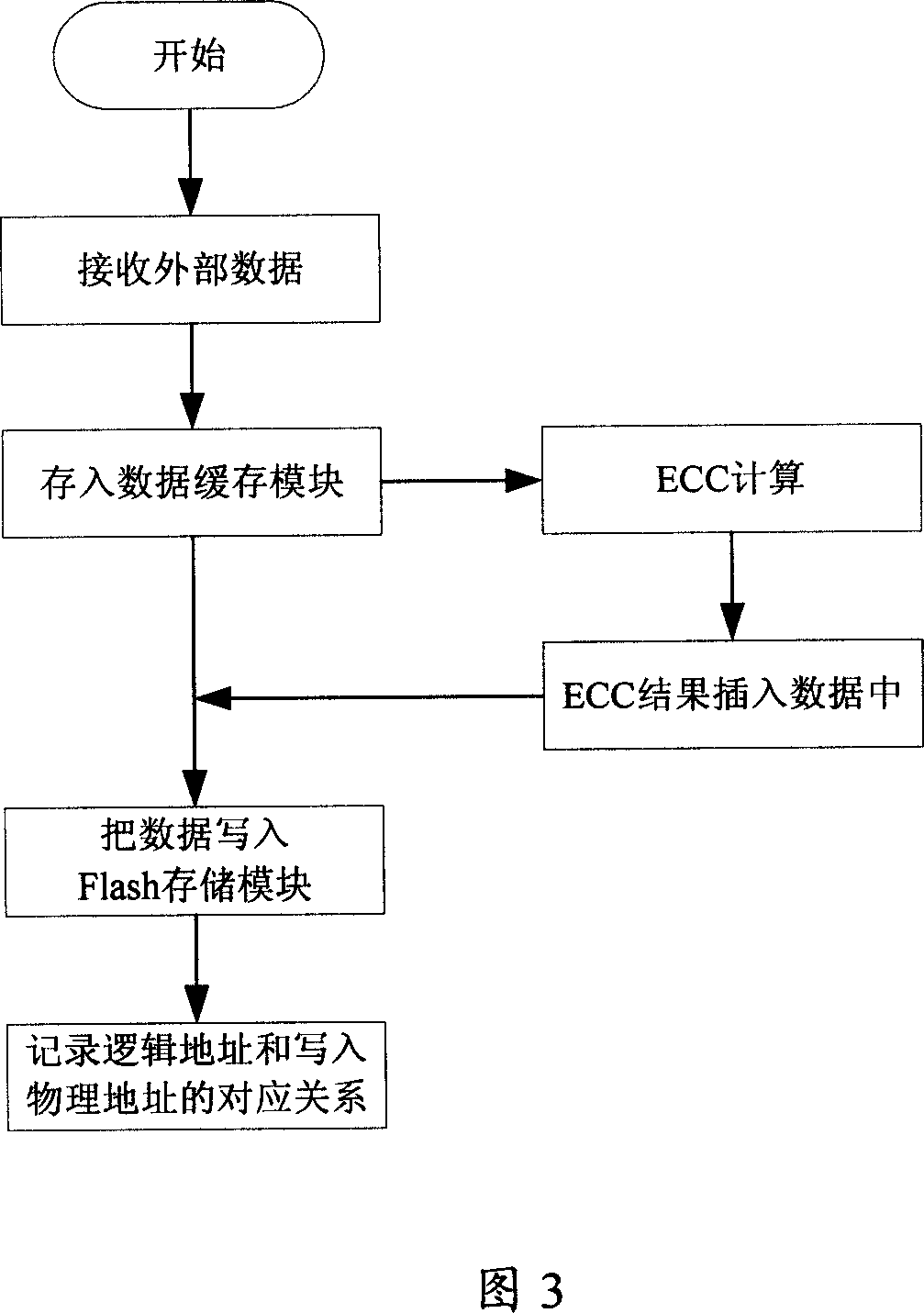
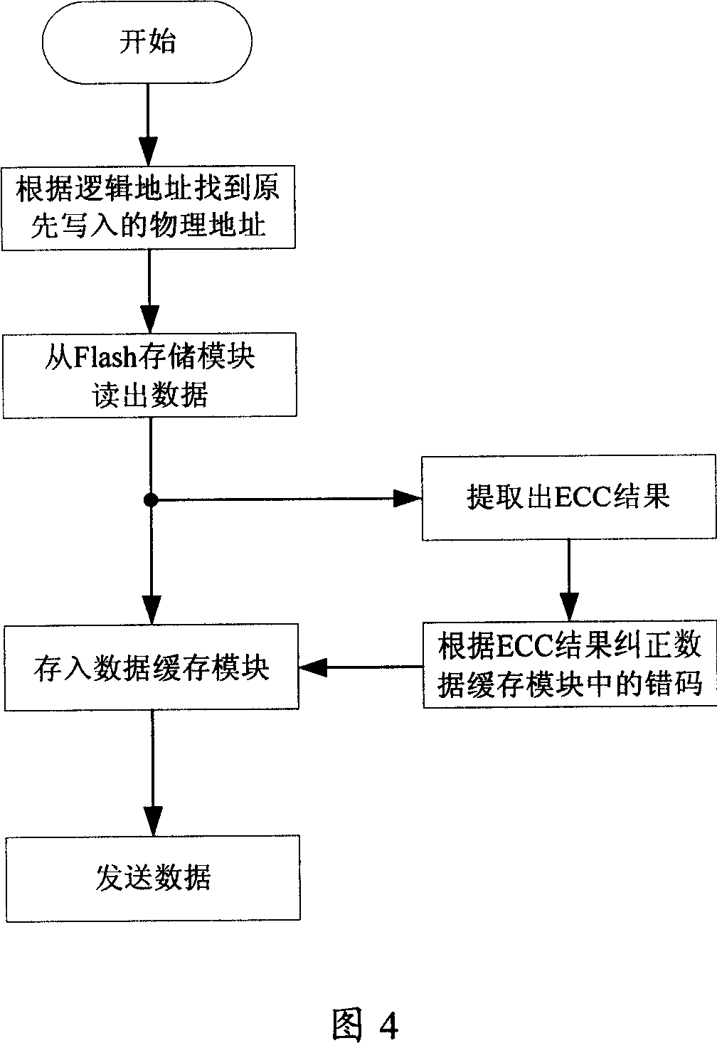
[0035] As shown in Figure 1, a kind of NAND FLASH storage device, comprises the NAND FLASH module 2 that is used to receive and store data, also integrates a management control module 1 on the storage device, one end of the management control module 1 passes through the FLASH bus and the NAND FLASH module 2 The other end is connected to the external application equipment through the external interface.

[0036] As shown in Figure 2, the management control module 1 is used to complete the command analysis of the external interface, the transmission and configuration of data between the external application device and the NAND FLASH module, the report of the running status, and also complete the reading of the NAND FLASH module. Operations such as writing, erasing, and backup are composed of an external interface module 11, a data cache module 12, a management algorithm and ECC module 13, and a NANDFLASH interface module 14.

[0037] The external interface interface 11 conforms ...


PUM


Abstract

The disclosed NAND FLASH memory device includes NAND FLASH module, and management control module integrated in the memory device. Through FLASH bus, one end of the management control module is connected to NAND FLASH module, and the other end is connected to external application device through external interface. The said management control module is composed of external interface module, data buffer module, management algorithm and ECC module, and NAND FLASH interface module. Comparing with general simplex NAND FLASH module, the disclosed NAND FLASH memory possesses features of simpler definition of interfaces, more diversified forms of application, simpler applications, and broadening range of NAND FLASH application.

Description

technical field [0001] The invention relates to a nonvolatile semiconductor storage device, in particular to a NAND FLASH storage device suitable for large-capacity data storage. Background technique [0002] NAND FLASH and NOR FLASH are the two main non-volatile flash memory technologies on the market today. Compared with the two, NOR FLASH is faster than NAND FLASH in random reading, but its capacity is small and the writing speed is slow. It is not suitable for large-capacity data storage and is mainly used for program code storage. NAND FLASH is widely used in the field of memory cards due to its advantages of large capacity, high-speed reading and writing, relatively low price, and suitable for large-capacity data storage. [0003] However, the operation of NAND FLASH is much more complicated than that of NOR FLASH, mainly in the following aspects: [0004] (1) NOR FLASH can be directly addressed through the address bus, and it is easy to read and write bytes. Its int...

Claims


Application Information

Patent Timeline
IPC IPC(8): G11C16/06G11C11/56G11C29/42
Inventor 骆建军楚传仁
Owner SAGE MICROELECTRONICS CORP
Learn More