Partition device and alignment method for wafer
A wafer and alignment mechanism technology, applied to fine working devices, electrical components, circuits, etc., can solve the problems of reduced productivity and long time, and achieve the effect of improving productivity
- Summary
- Abstract
- Description
- Claims
- Application Information
AI Technical Summary
Problems solved by technology
Method used
Image

Examples
Embodiment Construction
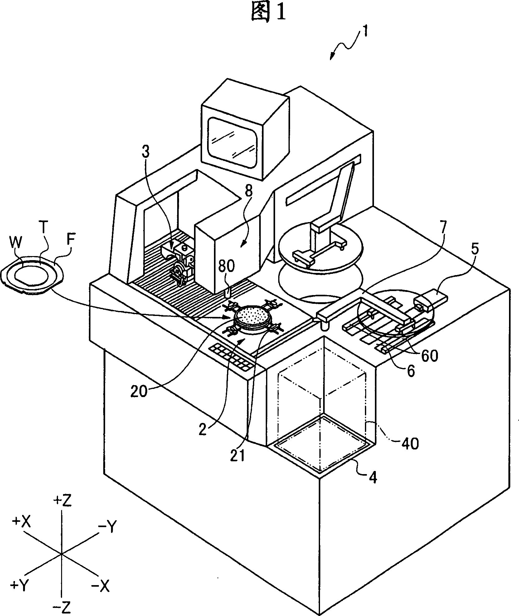
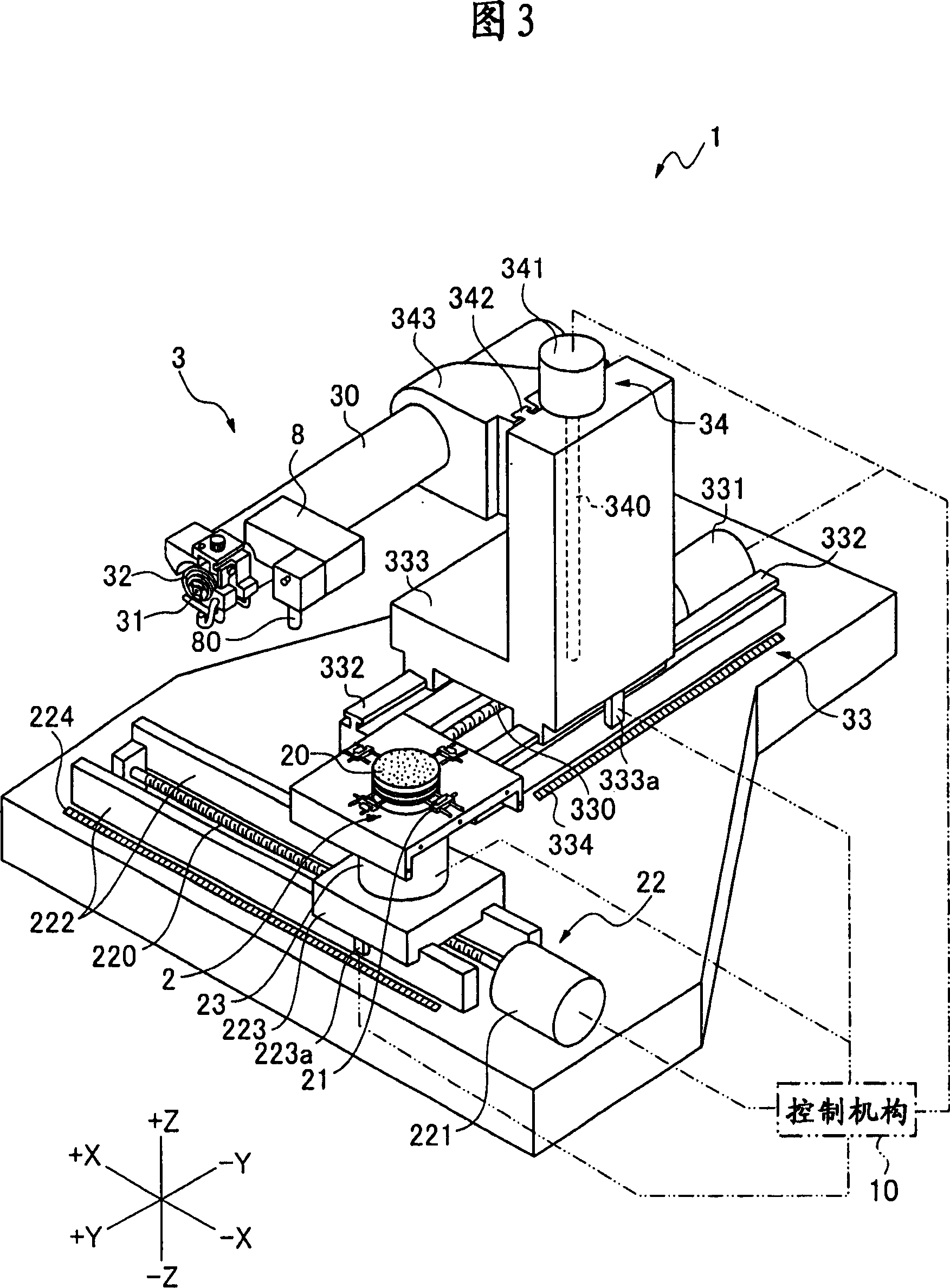
[0027] A cutting device 1 shown in FIG. 1 is a type of dividing device having a function of dividing a workpiece, and holds a workpiece on a chuck table 2 . The cutting mechanism 3 as a processing mechanism acts on the workpiece to cut it.
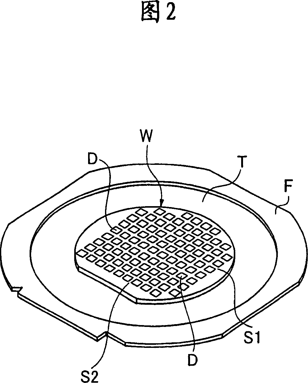
[0028] As shown in FIG. 2, on the surface of the workpiece, that is, the wafer W, a first planned separation line S1 and a second planned separation line S2 are formed orthogonally, and are divided by the first planned separation line S1 and the second planned separation line S2. And several devices D are formed. The wafer W is attached to a small piece of tape T, and the ring-shaped frame F is attached to the outer peripheral portion of the small piece of tape T, and the wafer W is integrally supported by the small piece of tape T and the frame F. .
[0029] A plurality of wafers W integrated with the frame F by the tape T in this way are housed in the wafer cassette 40 shown in FIG. The cassette mounting table 4 can be raised and lowe...
PUM
 Abstract
Description
Claims
Application Information
 - R&D
- Intellectual Property
- Life Sciences
- Materials
- Tech Scout
- Unparalleled Data Quality
- Higher Quality Content
- 60% Fewer Hallucinations
Browse by: Latest US Patents, China's latest patents, Technical Efficacy Thesaurus, Application Domain, Technology Topic, Popular Technical Reports.
© 2025 PatSnap. All rights reserved.Legal|Privacy policy|Modern Slavery Act Transparency Statement|Sitemap|About US| Contact US: help@patsnap.com