
Patsnap Eureka
For R&D, Patsnap Eureka makes reading and utilizing patents & technical documents easy.
Patsnap Eureka AIR
Designed for self-driven R&D workflows. Generate viable solutions, solve complex R&D challenges, empower your innovation with AI.

Patsnap Eureka Materials
Designed for material experts only. Revolutionize your material R&D, from search, analyze, to developing new materials.

TechResearch
Generate reliable direction feasibility study reports for your R&D in just a few steps.

TechSeek
Discover and master advanced knowledge NOW. Basics, ideas, possibilities, all at once.

TechMind
As an expert in R&D Theories, TechMind can generates customized viable solutions instantly.

TechRisk
Analyze your overall solution with one click, know your potential R&D risks in advance.

TechMonitor
Get weekly tech updates, stay abreast of the latest tech innovations and key insights.
High-energy electron-diffraction diagram processing system and method
A high-energy electron diffraction and image processing technology, applied in electrical digital data processing, chemical instruments and methods, and input/output process of data processing, etc. Effect
- Summary
- Abstract
- Description
- Claims
- Application Information
AI Technical Summary
Problems solved by technology
Method used
Image


Examples
Embodiment Construction
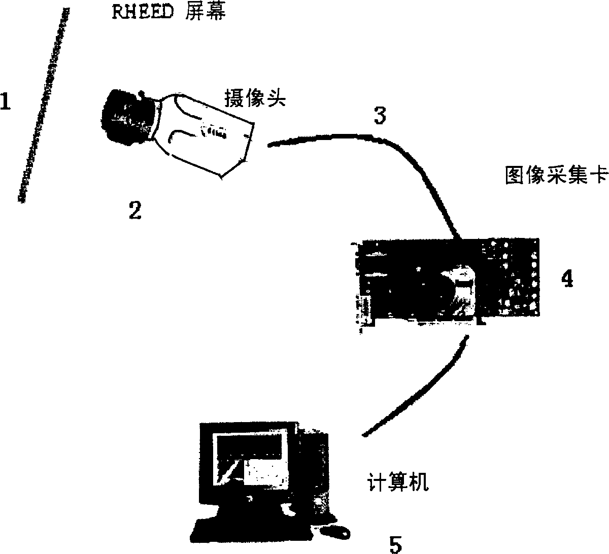
[0035] see figure 2 , figure 2 It is a connection diagram of each component of the system. A high-energy electron diffraction image processing system of the present invention is characterized in that it includes:
[0036] A high-energy electron diffraction fluorescent screen 1;
[0037] A CCD camera 2, the CCD camera 2 is placed behind the high-energy electron diffraction fluorescent screen 1, and the CCD camera is fixed with a stainless steel cylinder;
[0038] An image acquisition card 4, the image acquisition card 4 is connected with the CCD camera 2 with the video line 3, and the image acquisition card 4 converts the analog signal obtained by the CCD camera 2 into a digital signal, and stores it in the memory;
[0039] A computer 5, the computer 5 is connected with the image acquisition card 4 with the video line 3, the computer 5 processes the data in the internal memory, and images the data on the screen of the computer 5.
[0040] 2. A high-energy electron diffract...
PUM
 Abstract
Description
Claims
Application Information
 - R&D Engineer
- R&D Manager
- IP Professional
- Industry Leading Data Capabilities
- Powerful AI technology
- Patent DNA Extraction
Browse by: Latest US Patents, China's latest patents, Technical Efficacy Thesaurus, Application Domain, Technology Topic, Popular Technical Reports.
© 2024 PatSnap. All rights reserved.Legal|Privacy policy|Modern Slavery Act Transparency Statement|Sitemap|About US| Contact US: help@patsnap.com