Driving method of display device
A driving method and technology for display devices, which are applied to static indicators, cathode ray tube indicators, instruments, etc., can solve problems such as video signals cannot be accurately input, low image display quality, etc., achieve good image display, simplify peripheral The effect of the circuit structure
- Summary
- Abstract
- Description
- Claims
- Application Information
AI Technical Summary
Problems solved by technology
Method used
Image
Examples
Embodiment approach 1
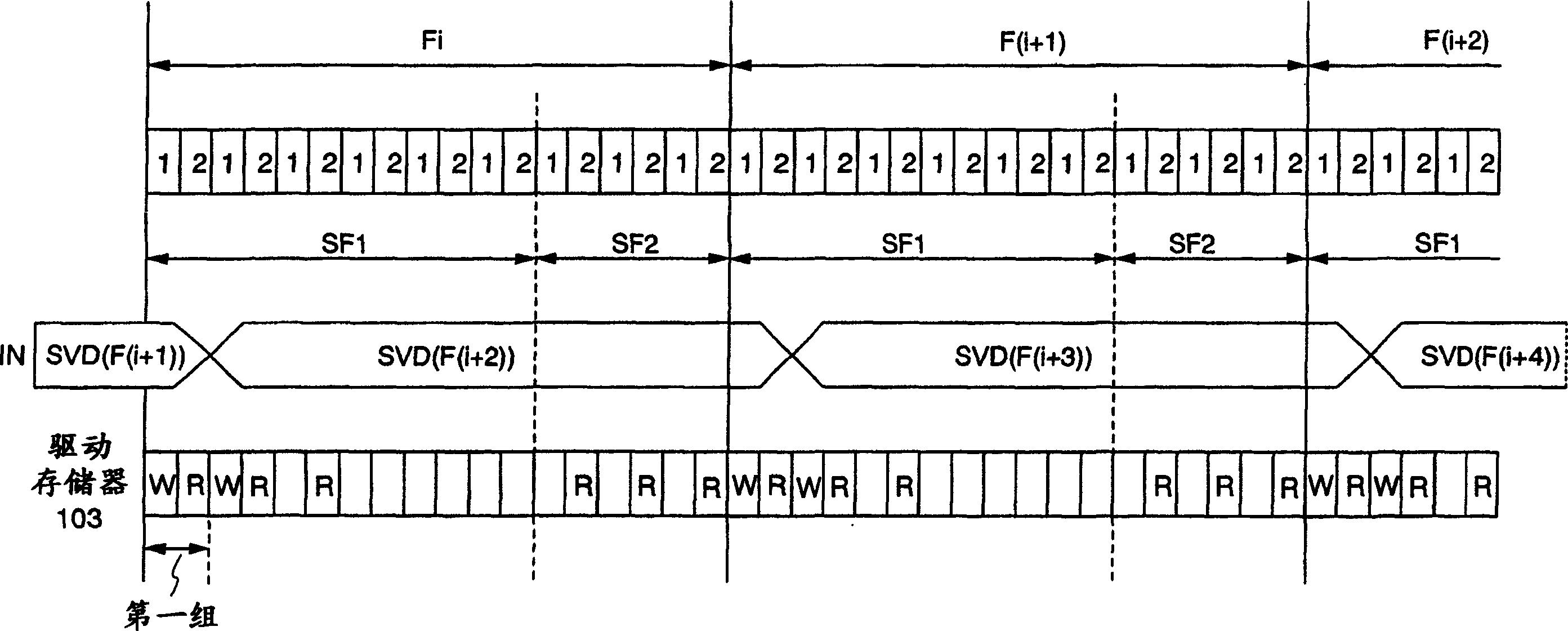
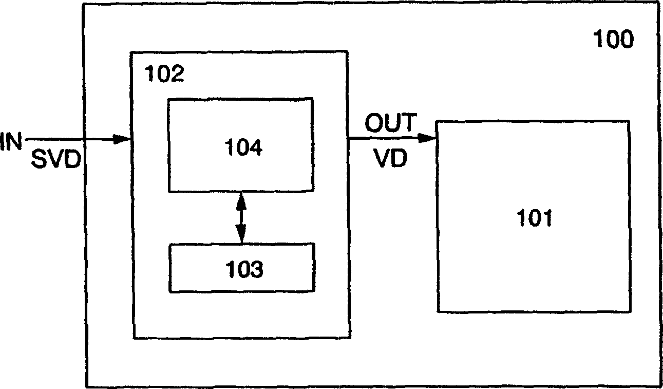
[0033] will refer to figure 1 , 2A Embodiment 1 is described with 2B. figure 1 is a timing chart showing a driving method of the display device. Figure 2A and 2B shows the use of figure 1 The timing diagram shown in the drive method shows the structure of the device.
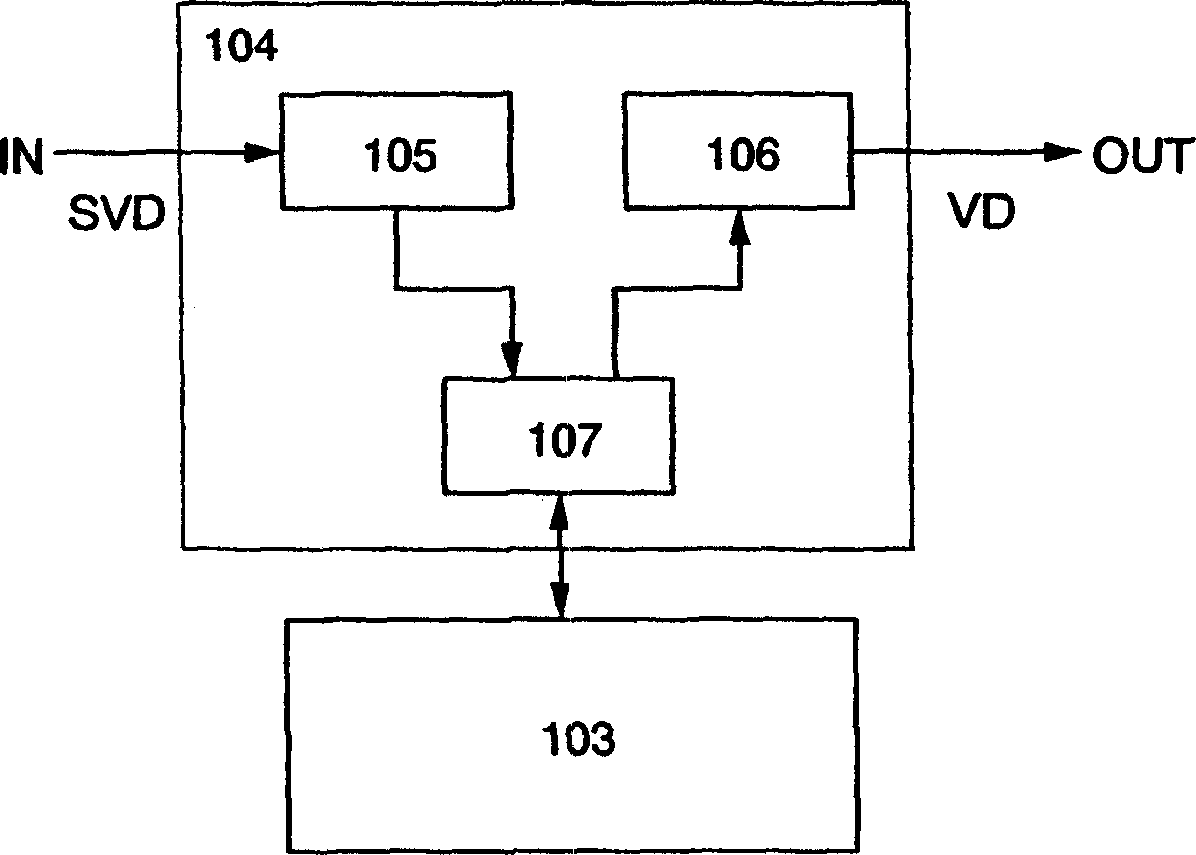
[0034] exist Figure 2A Among them, a display device 100 includes a panel 101 and a peripheral circuit 102 . The peripheral circuit 102 includes a controller 104 and a memory 103 . The source video signal SVD input into the display device is input into the peripheral circuit 102 (in Figure 2A is indicated by "IN"). The source video signal SVD input into the peripheral circuit 102 is written into the memory 103 through the controller 104 . The video signal written in the memory 103 is read out by the controller 104 and output from the peripheral circuit 102 as a video signal VD (in Figure 2A is indicated by "OUT"). A video signal VD is input into panel 101 . Panel 101 performs image display using v...
Embodiment approach 2
[0054] The following will refer to Figure 3A , 3B and Figure 4 A description of Embodiment Mode 2 is made. Figure 3A and 3B Shown is a more specific structure of the memory 103 in the display device shown in FIG. 2, and the driven state of the memory 103 in each of two consecutive frame periods Fi and F(i+1). Figure 4 is shown in use Figure 3A and 3B The timing chart of the driving method of the display device in the case of the memory shown in FIG. 2 as the memory 103. It should be noted that, figure 1 and Figure 4 Common parts among them are denoted by common reference numerals, and descriptions thereof will be omitted.
[0055] Such as Figure 3A and 3B As shown in , the memory 103 has a first memory area 301 and a second memory area 302 . Each of the first memory area 301 and the second memory area 302 has a storage capacity capable of storing video signals corresponding to a plurality of pixels in the panel 101 .
[0056] During the frame period Fi, the ...
Embodiment approach 3
[0062] In Embodiment 3, reference will be made to Figure 5A and 5B A description is made of an example of the panel 101 in FIG. 2 . exist Figure 5A , the panel 101 has a pixel portion 501 including a plurality of pixels 500 arranged in a matrix. The pixel portion 501 may have an active matrix arrangement in which a switching element such as a thin film transistor is provided in each pixel 500 . As a display element of the pixel 500 , a light emitting element such as an electroluminescent element may be provided or a liquid crystal element may be provided.
[0063] It should be noted that if Figure 5B As shown in , a driver circuit for driving the pixel portion 501 may be provided on the same substrate as the pixel portion 501 . It should be noted that, Figure 5A and 5B Common parts therebetween are denoted by common reference numerals, and descriptions thereof will be omitted. exist Figure 5B In , the first driver circuit 503 and the second driver circuit 504 are...
PUM
 Abstract
Description
Claims
Application Information
 - R&D Engineer
- R&D Manager
- IP Professional
- Industry Leading Data Capabilities
- Powerful AI technology
- Patent DNA Extraction
Browse by: Latest US Patents, China's latest patents, Technical Efficacy Thesaurus, Application Domain, Technology Topic, Popular Technical Reports.
© 2024 PatSnap. All rights reserved.Legal|Privacy policy|Modern Slavery Act Transparency Statement|Sitemap|About US| Contact US: help@patsnap.com


