Solid-state image sensor

A technology of a solid-state imaging device and an imaging unit, which is applied in the direction of electric solid-state devices, radiation control devices, image communication, etc., and can solve problems such as the deterioration of electron transmission efficiency

Inactive Publication Date: 2006-04-19
SANYO ELECTRIC CO LTD
View PDF1 Cites 0 Cited by
  • Summary
  • Abstract
  • Description
  • Claims
  • Application Information

AI Technical Summary

Problems solved by technology

Thus, there is a disadvantage that electrons stored in the n-type impurity region 408 under the transfer electrode 404 in the on state adjacent to the transfer direction side of the transfer electrode 404 in the off state are transferred beyond the transfer in the off state. The potential of the n-type impurity 408 under the electrode 404 flows out to the n-type impurity region 408 under the on-state transfer electrode 404 on the opposite side to the transfer direction.
Therefore, there is a problem that the transfer efficiency of electrons deteriorates

Method used


Image

  • Solid-state image sensor
  • Solid-state image sensor
  • Solid-state image sensor

Examples


Embodiment Construction

[0042] Embodiments of the present invention will be described below according to the accompanying drawings.

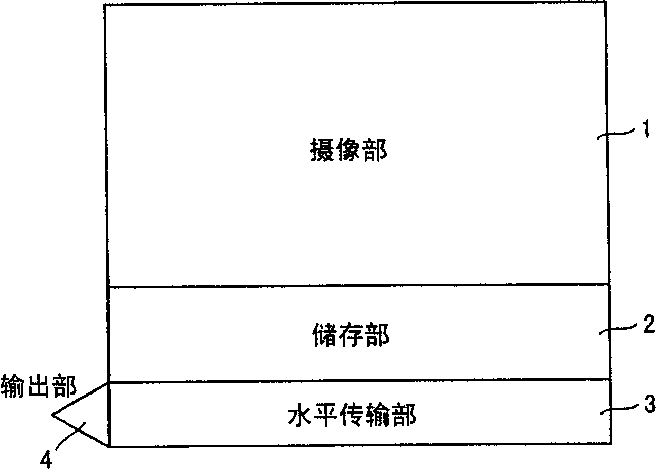
[0043] refer to Figure 1 ~ Figure 4 , in this embodiment mode, an example in which the present invention is applied to a frame transfer type solid-state imaging device will be described.

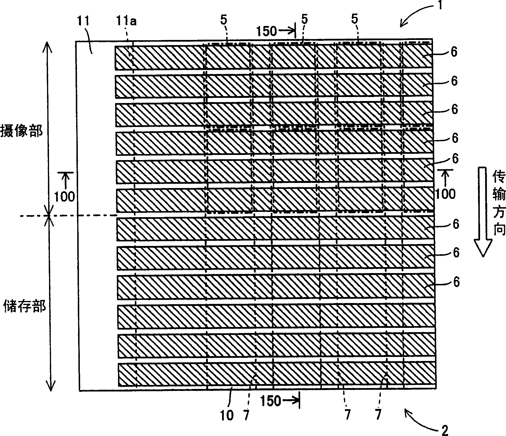
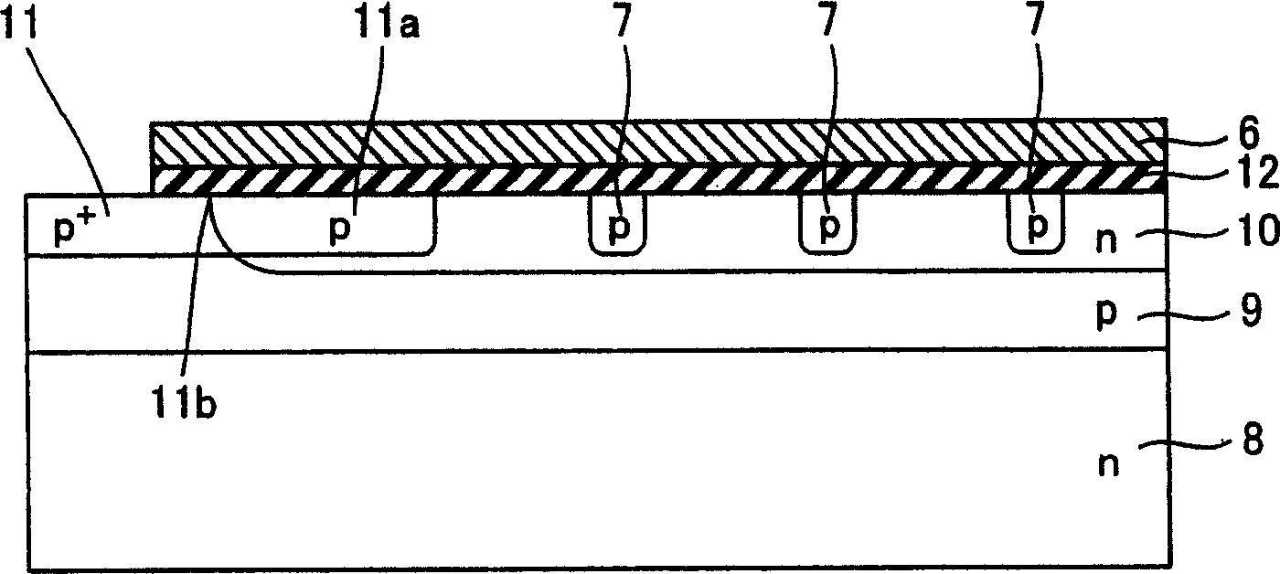
[0044] The frame transfer type solid-state imaging device of this embodiment, such as figure 1 As shown, it includes: an imaging unit 1 , a storage unit 2 , a horizontal transmission unit 3 and an output unit 4 . The imaging unit 1 is provided to perform photoelectric conversion by utilizing incident light. In addition, the imaging unit 1 such as figure 2 As shown, there is a configuration in which a plurality of pixels 5 having a photoelectric conversion function are arranged in a matrix. In addition, the imaging unit 1 has a function of storing the generated electrons and holes and transferring them to the storage unit 2 . In addition, a part of the holes stored in the imag...


PUM


Abstract

A solid-state image sensor capable of suppressing deterioration of a transfer efficiency of electrons is provided. The solid-state image sensor comprises a first conductive type first impurity region that can store electrons and holes; a second conductive type second impurity region that is formed so as to have a region where the first and second impurity regions overlap one another; and a transfer electrode that is formed to overlie and extend at least from the first impurity region to the region where the first and second impurity regions overlap one another.

Description

technical field [0001] The present invention relates to a solid-state imaging device, and more particularly, to a solid-state imaging device having a transfer electrode. Background technique [0002] Conventionally, various solid-state imaging devices including transfer electrodes are known. Such a solid-state imaging device is disclosed in Japanese Unexamined Patent Publication No. 2001-156284, for example. [0003] Figure 12 It is a plan view for explaining the configuration of an imaging unit and a storage unit of a conventional solid-state imaging device including a transfer electrode. Figure 13 for along Figure 12 A cross-sectional view taken along line 500-500 of a conventional solid-state imaging device shown as an example. refer to Figure 12 , the solid-state imaging device of an example in the past includes: the imaging part 401 that carries out photoelectric conversion by the incident of light; Transmitter (not shown in the figure). The imaging unit 401 has...

Claims


Application Information

Patent Timeline
Patent Type & Authority Applications(China)
IPC IPC(8): H01L29/762H01L27/146H04N5/335H01L27/148
CPCH01L27/1485H01L29/76883
Inventor 海田孝行
Owner SANYO ELECTRIC CO LTD
Why Eureka
Try Eureka