Method for producing multicrystalline silicon layer

A technology of polysilicon layer and polysilicon, which is applied in semiconductor/solid-state device manufacturing, electrical components, circuits, etc., can solve the problems of reducing the electron mobility of the channel layer and affecting the electrical quality of LTPSTFT, etc.

Active Publication Date: 2005-03-02
AU OPTRONICS CORP
View PDF1 Cites 14 Cited by
  • Summary
  • Abstract
  • Description
  • Claims
  • Application Information

AI Technical Summary

Problems solved by technology

However, the polysilicon layer 14 as the channel layer of the device contains a grain boundary corresponding to the thin amorphous silicon region 13b and the remaining thick

Method used


Image

  • Method for producing multicrystalline silicon layer
  • Method for producing multicrystalline silicon layer
  • Method for producing multicrystalline silicon layer

Examples


Embodiment Construction

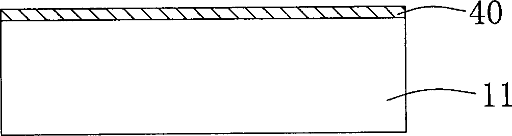
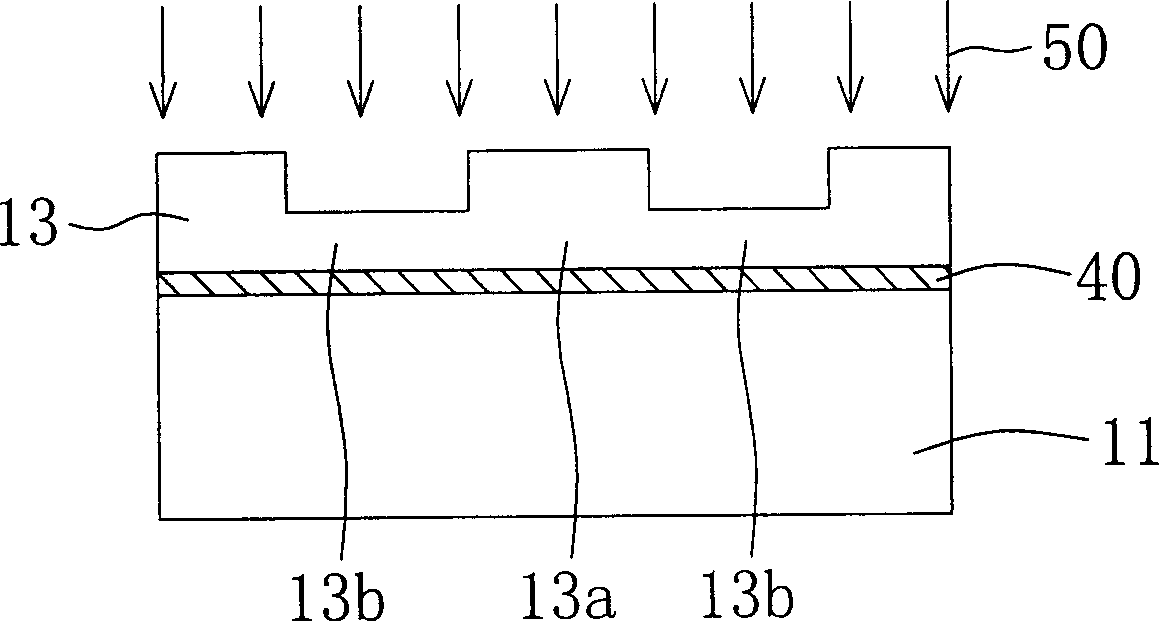
[0018] Please refer to Figure 2A-2D , which is a flow sectional view of a method for manufacturing a polysilicon layer according to a preferred embodiment of the present invention. First, in Figure 2A In the present invention, a substrate 111 is provided, and an insulating layer 140 is formed on the substrate 111 . In this embodiment, the substrate 111 is, for example, a glass substrate or a plastic substrate, and the insulating layer 140 is, for example, a silicon dioxide (SiO2) 2 ) layer, a silicon nitride layer or a nitride layer. Then, if Figure 2B As shown, an amorphous silicon (amorphous silicon, α-Si) layer 113 is formed on the insulating layer 140 . The amorphous silicon layer 113 has at least one thick amorphous silicon region 113a and one thin amorphous silicon region 113b, and the thick amorphous silicon region 113a and the thin amorphous silicon region 113b respectively have a first thickness H1 and a second thickness H2. The first thickness H1 is greater t...


PUM


Abstract

The method includes the steps: 1) to from a insulating layer on a base board, 2) to form an amorphous silicon layer on the insulating, layer, the amorphous silicon layer includes a amorphous silicon thick area and a amorphous silicon thin area, 3) to fully melt the amorphous silicon layer to a first molten state amorphous silicon area that center of the bottom is corresponding to center of bottom of the amorphous silicon thick area and a second molten state amorphous silicon area that center of the bottom is corresponding to center of the amorphous silicon thin area. The temp. of first molten state amorphous silicon area is lower than the temp. of second molten state amorphous silicon area. Finally, to crystallize from first molten state amorphous silicon area to second molten state amorphous silicon area, thus to form polysilicon layer.

Description

technical field [0001] The present invention relates to a method for manufacturing a polysilicon layer, and in particular to a method for laterally crystallizing a thick amorphous silicon region and a thin amorphous silicon region to form a polysilicon layer. Background technique [0002] In today's era of rapid technological development, display panels have been widely used in portable electronic devices such as notebook computers, personal digital assistants, and mobile phones. Among them, the display panel can be divided into a non-polysilicon (amorphous silicon, α-Si) thin film transistor (thinfilm transistor, TFT) display panel and a low temperature polysilicon (LTPS) TFT display panel. The biggest difference between the LTPS TFT display panel and the α-Si TFT display panel is that the LTPS TFT display panel converts the α-Si layer into a polysilicon layer by laser annealing (Laser Annealing), which greatly improves the electron mobility (electron mobility) of the thin ...

Claims


Application Information

Patent Timeline
IPC IPC(8): H01L21/00H01L21/20H01L21/36
Inventor 陈亦伟张志雄许宗义
Owner AU OPTRONICS CORP
Why Eureka
Try Eureka