Module component

A technology for module components and components, which is applied in the fields of semiconductor/solid-state device components, electrical components, and electrical solid-state devices, and can solve the problems of overall performance impact and reliability damage of packaged components.

Inactive Publication Date: 2005-02-09
FUJITSU MEDIA DEVICES
View PDF1 Cites 2 Cited by
  • Summary
  • Abstract
  • Description
  • Claims
  • Application Information

AI Technical Summary

Problems solved by technology

As a result, the overall performance of the packaged components suffers and reliability is compromised

Method used


Image

  • Module component
  • Module component
  • Module component

Examples


Embodiment Construction

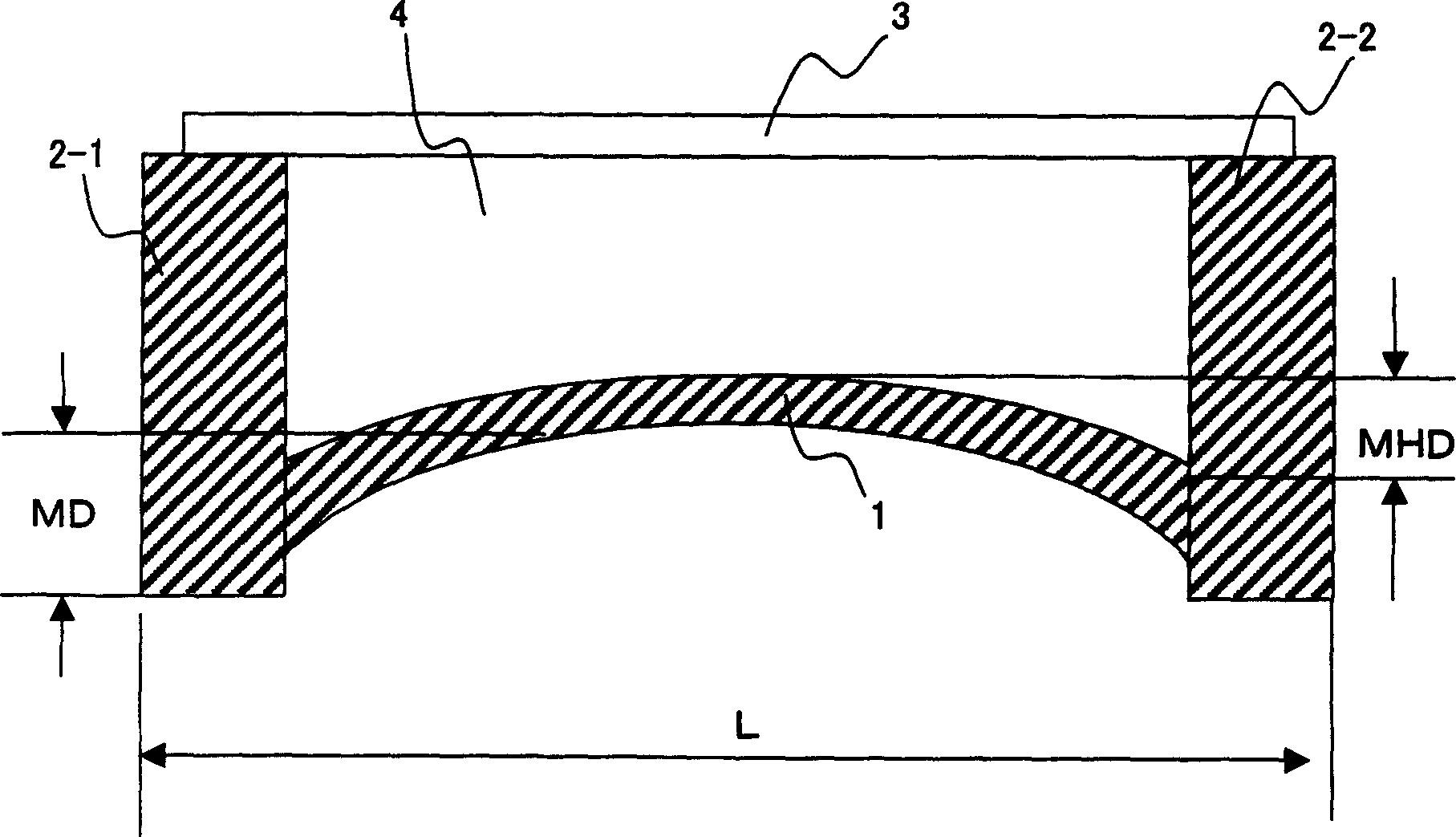
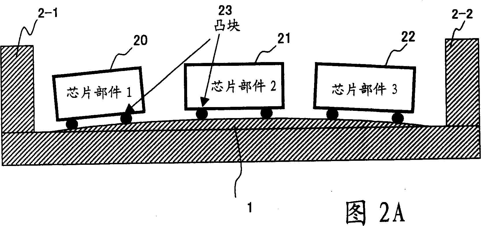
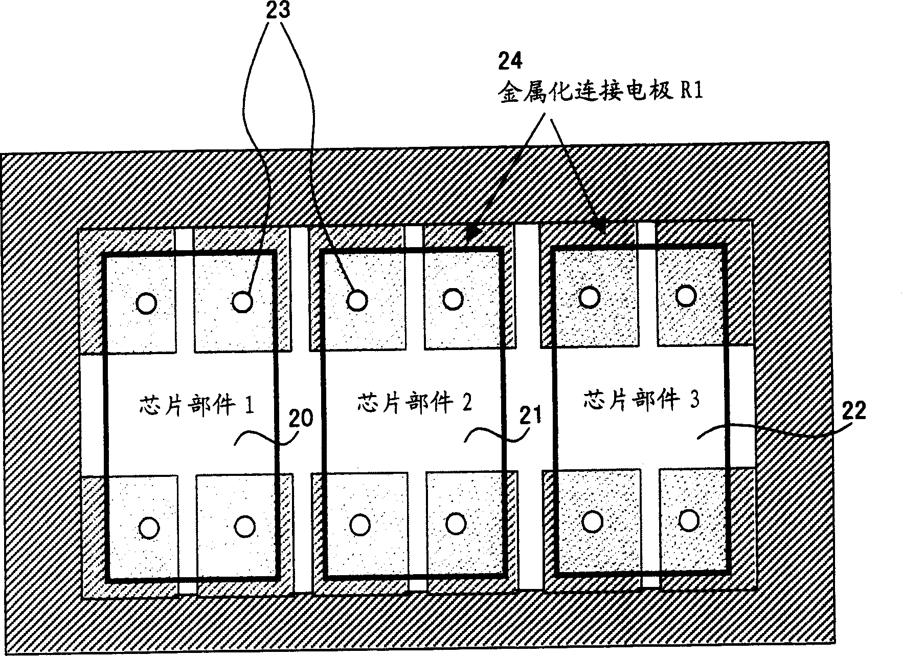
[0025] Figure 3 shows a first embodiment of the present invention. FIG. 3A is a cross-sectional view of the chip carrier with the cover 3 removed. Figure 3B is a top view of the chip carrier. Two chip components 20 , 21 are mounted on the chip carrier substrate 1 .

[0026] This embodiment is characterized in that the dimensions of the bumps 23-1, 23-2, which connect the plurality of chip components 20, 21 to the metal connected to the electrode 24.

[0027] More specifically, in the embodiment shown in FIG. 3 , a connection electrode 24 is metallized on the substrate 1 , and a plurality of chip components (two chip components in the case of FIG. 3 ) 20, 21 pass through bumps 23 -1, 23-2 are mounted on the connection electrode 24.

[0028] In addition, on the basis of the height of the bump 23-1 in the central area of ​​the substrate 1 in the length direction of the substrate 1 (that is, the lateral direction in the figure), the bump (bump 23-1) is placed in the direction ...


PUM


Abstract

A module device with mounted components with no damage in reliability. This device has a board with metallized connection electrodes and components mounted on the board by arrangement in the longitudinal direction of the board, and each connected to the connection electrode via a bump. Bumps for connecting the components to the board connection electrodes are so set that their height may increase toward the side of the board with the reference of the height of the bump located at the center region in the longitudinal direction of the board.

Description

technical field [0001] The present invention relates to a module part on which a part such as a surface acoustic wave element is mounted and sealed. Background technique [0002] With the continuous miniaturization of electronic equipment in recent years, it is necessary to mount small and thin electronic components on these electronic equipment, especially cellular phones. Meanwhile, for ease of production and miniaturization, a module part in which a plurality of chip parts are mounted on one package is used. [0003] figure 1 Shown is a cutaway view of the module part package. This package has a chip carrier consisting of a chip-carrier substrate 1 and chip-carrier walls (encapsulated chips) 2-1, 2-2, in which a plurality of electronic components are accommodated. In addition, a plurality of chip components are accommodated in the package space 4 and are sealed by the cover 3 . [0004] The chip carrier is made of sintered aluminum oxide layer, and there are electrode...

Claims


Application Information

Patent Timeline
IPC IPC(8): H01L25/18H01L21/60H01L23/02H01L23/08H01L23/48H01L23/485H01L25/04H03H9/25
CPCH01L2924/14H01L24/10H01L2924/01058H01L2224/13099H01L2924/01013H01L2224/16H01L2224/0401H01L2224/16225H01L2224/1403H01L2924/15151H01L2924/3511H01L2924/01004H01L2924/16195H01L2924/01006H01L2924/01033H01L2224/0603H01L24/13H01L2924/15787H01L2224/13H01L2924/00H01L23/12H03H9/25H01L23/50
Inventor 宫地直已黑川顺子
Owner FUJITSU MEDIA DEVICES
Why Eureka
Try Eureka