Glow organic electroluminescent device and manufacturing method thereof
An electroluminescence and device technology, which is applied in the field of red light organic electroluminescence devices and their manufacturing, can solve the problems of not being substantially improved, and achieve the effects of improving electroluminescence performance, high efficiency, and high color purity
- Summary
- Abstract
- Description
- Claims
- Application Information
AI Technical Summary
Problems solved by technology
Method used
Image
Examples
Embodiment 1
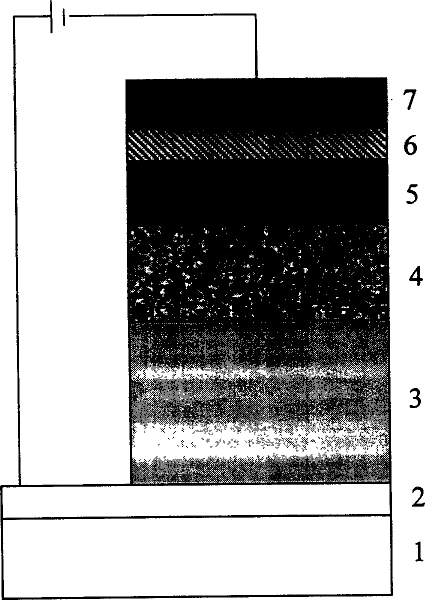
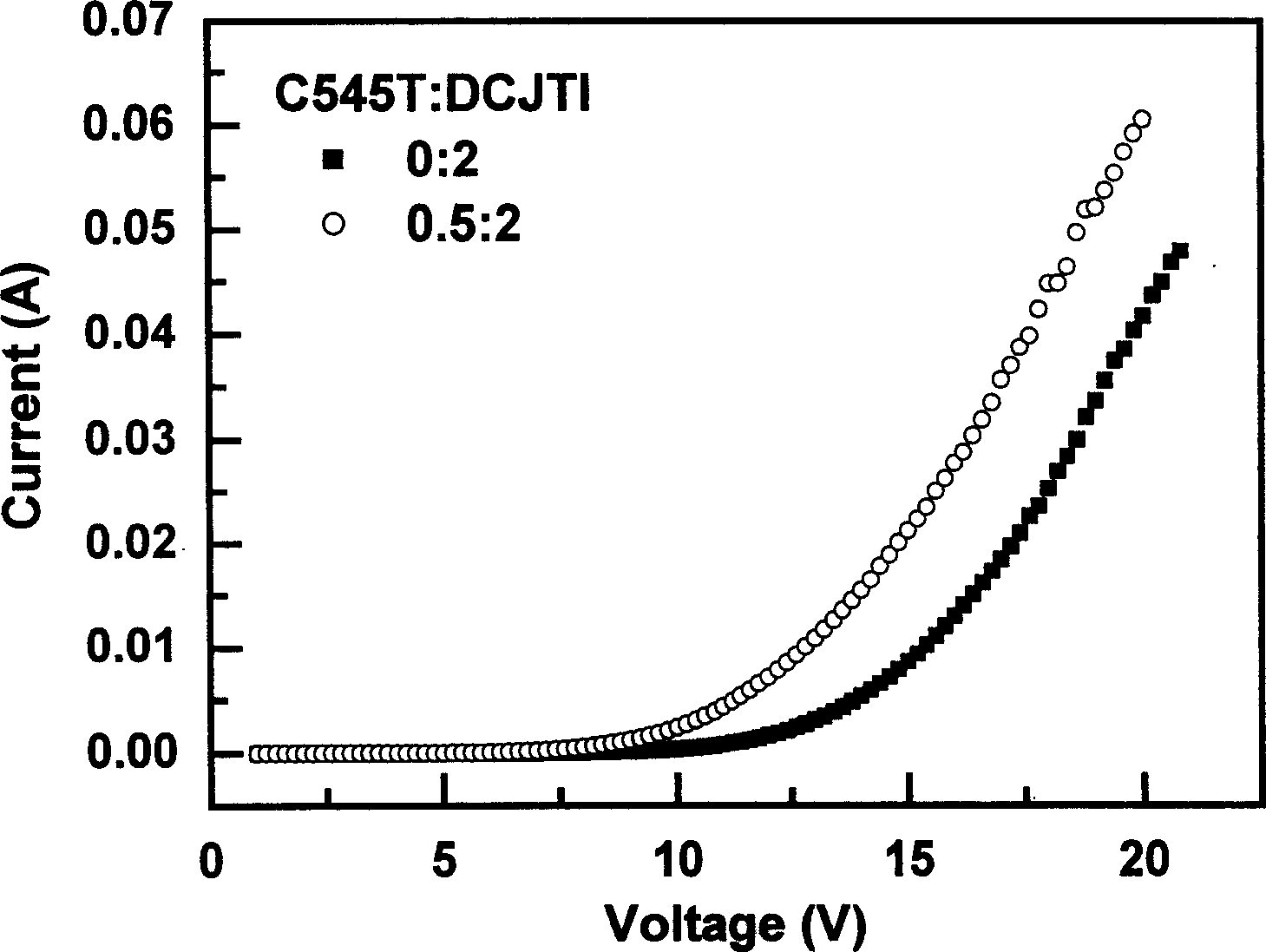
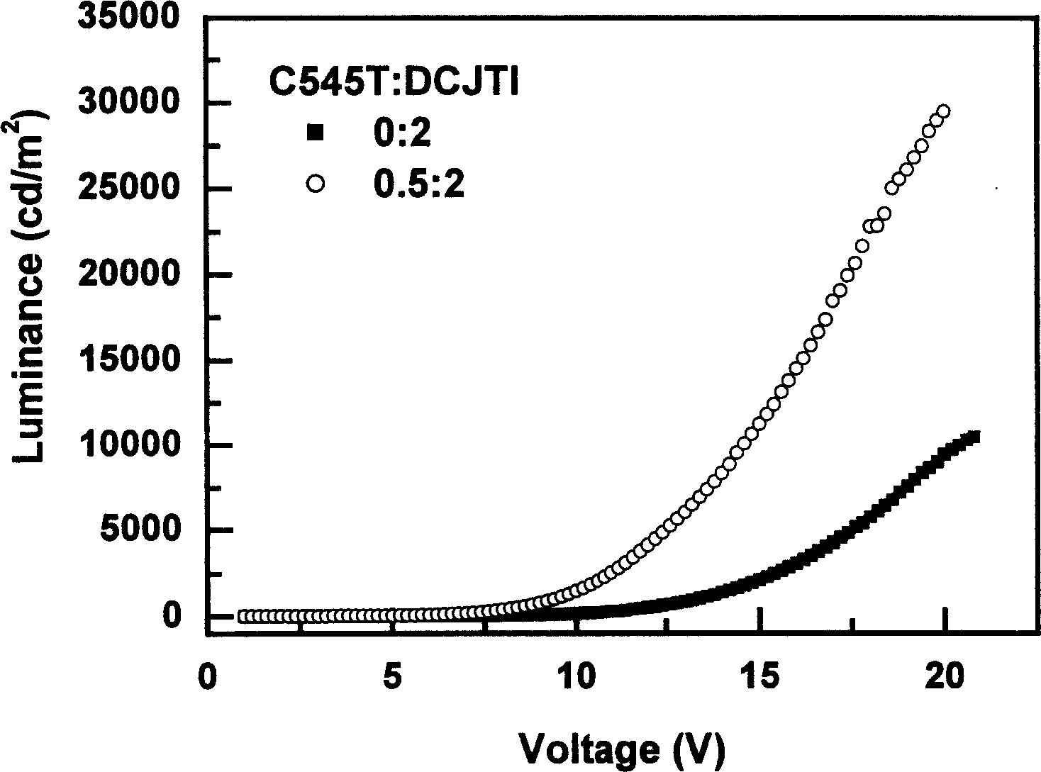
[0033] Doping of C545T and DCJTI to Alq 3 As the light-emitting layer, the structure is ITO / NPB / Alq 3 :C545T:DCJTI / Alq 3 / LiF / Al electroluminescent devices. at 10 -4 The organic and metal electrode layers are evaporated under a vacuum of Pa. The evaporation rate of the organic layer is controlled at 0.1-4 Å / s, the evaporation rate of LiF is controlled at 0.2 Å / s, and the evaporation rate of the metal is controlled at 5 Å / s. Alq 3 The doping concentration ratio of :C545T:DCJTI is controlled at 1:0.5%:2%. Among them, the thickness of the NPB layer is 50nm, the doped light-emitting layer is 30nm, Alq 3 The layer is 20nm, the LiF layer is 1nm, and the Al layer is 100nm. The obtained device is driven by DC voltage, and the red light emission of DCJTI can be obtained, the maximum power efficiency is 9.4lm / W, the maximum current efficiency is 11.2cd / A, and the maximum brightness can reach 29500cd / m 2 , the main peak of luminescence is 615nm. Under the same conditions, the maxi...
Embodiment 2
[0035] Doping of C545T and DCJTI to Alq 3 As the light-emitting layer, the structure is ITO / NPB / Alq 3 :C545T:DCJTI / Alq 3 / LiF / Al electroluminescent devices. at 10 -4 The organic and metal electrode layers are evaporated under a vacuum of Pa. The evaporation rate of the organic layer is controlled at 0.1-4 Å / s, the evaporation rate of LiF is controlled at 0.2 Å / s, and the evaporation rate of the metal is controlled at 5 Å / s. Alq 3 The doping concentration ratio of :C545T:DCJTI is controlled at 1:0.5%:1%. Among them, the thickness of the NPB layer is 50nm, the doped light-emitting layer is 30nm, Alq 3 The layer is 20nm, the LiF layer is 1nm, and the Al layer is 100nm. The obtained device is driven by DC voltage, and the red light emission of DCJTI can be obtained, the maximum power efficiency is 8.9lm / W, the maximum current efficiency is 12.6cd / A, and the maximum brightness can reach 33200cd / m 2 , the main peak of luminescence is 607nm. Under the same conditions, the max...
Embodiment 3
[0037] Doping of C545T and DCJTB into Alq 3 As the light-emitting layer, the structure is ITO / NPB / Alq 3 :C545T:DCJTB / Alq 3 / LiF / Al electroluminescent devices. at 10 -4 The organic and metal electrode layers are evaporated under a vacuum of Pa. The evaporation rate of the organic layer is controlled at 0.1-4 Å / s, the evaporation rate of LiF is controlled at 0.2 Å / s, and the evaporation rate of the metal is controlled at 5 Å / s. Alq 3 The doping concentration ratio of :C545T:DCJTB is controlled at 1:0.5%:0.5%. Among them, the thickness of the NPB layer is 50nm, the doped light-emitting layer is 30nm, Alq 3 The layer is 20nm, the LiF layer is 1nm, and the Al layer is 100nm. The obtained device is driven by DC voltage, and the red light emission of DCJTB can be obtained, the maximum power efficiency is 10.9lm / W, the maximum current efficiency is 11.7cd / A, and the maximum brightness can reach 23700cd / m 2 , the main peak of luminescence is 612nm. Under the same conditions, th...
PUM
 Abstract
Description
Claims
Application Information
 - R&D Engineer
- R&D Manager
- IP Professional
- Industry Leading Data Capabilities
- Powerful AI technology
- Patent DNA Extraction
Browse by: Latest US Patents, China's latest patents, Technical Efficacy Thesaurus, Application Domain, Technology Topic, Popular Technical Reports.
© 2024 PatSnap. All rights reserved.Legal|Privacy policy|Modern Slavery Act Transparency Statement|Sitemap|About US| Contact US: help@patsnap.com


