Electric erasing programmable logic element
A programming logic and electric erasing technology, which is applied to electrical components, electrical solid-state devices, circuits, etc., can solve the problem of large area of single-layer polysilicon storage cells
- Summary
- Abstract
- Description
- Claims
- Application Information
AI Technical Summary
Problems solved by technology
Method used
Image
Examples
Embodiment Construction
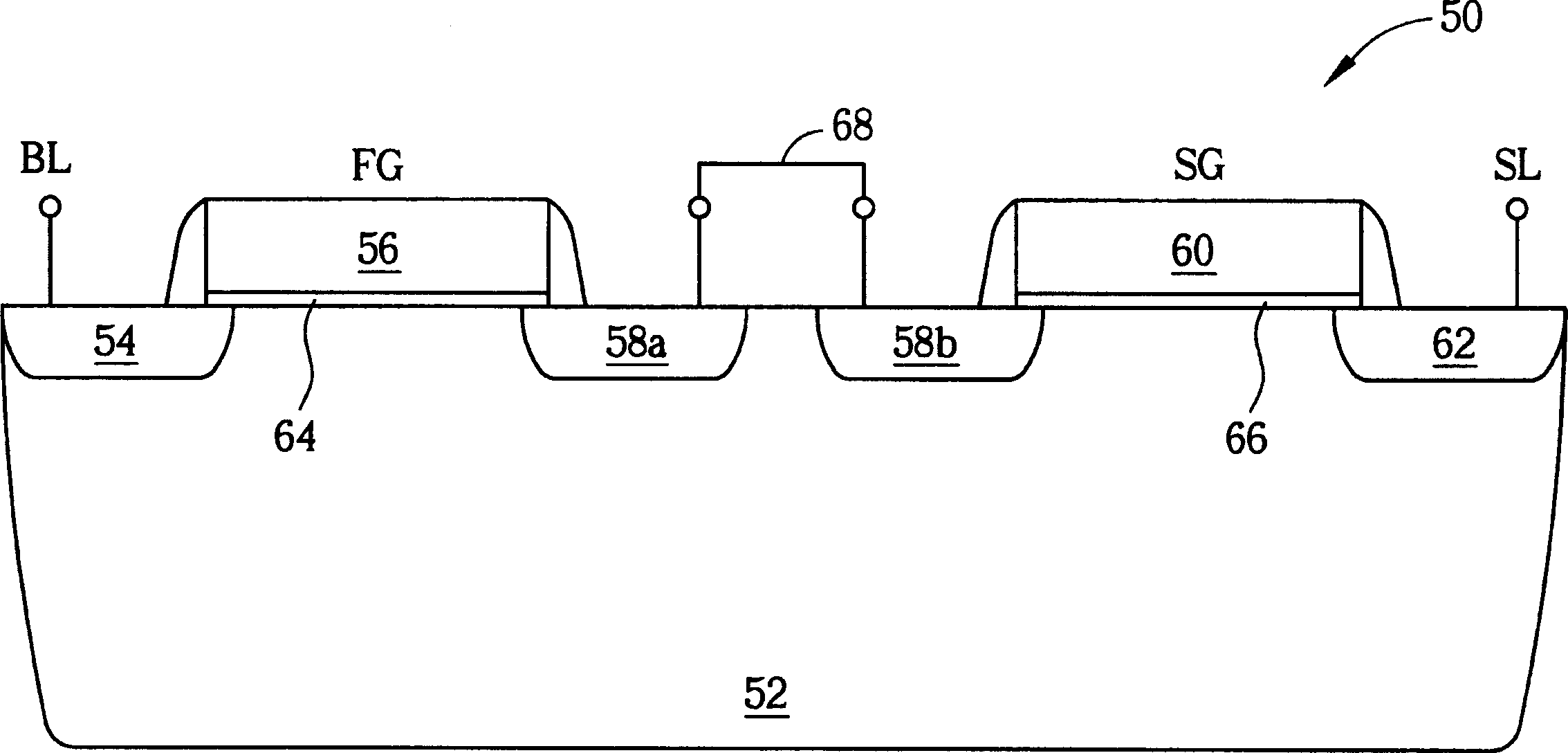
[0022] see figure 2 , figure 2 A front sectional view of an Electrically Erasable Programmable Logic Device (Electrically Erasable Programmable Logic Device) 50 of the present invention is shown in FIG. The electrically erasable programmable logic element 50 includes a P-type substrate (P-Type Substrate) 52; a first N-type ion-doped region 54, located in the P-type substrate 52; a first gate 56, which Located above the P-type substrate 52 and adjacent to the first N-type ion-doped region 54, and in a floating (Floating) state, used as a floating gate of the electrically erasable programmable logic element 50 to store The nonvolatile data of the electrically erasable programmable logic element 50; a second N-type ion-doped region 58a, located in the P-type substrate 52 and adjacent to the first grid 56; a third N-type The ion-doped region 58b is located in the P-type substrate 52 and is electrically connected to the second N-type ion-doped region 58b; a second gate 60, whic...
PUM
 Abstract
Description
Claims
Application Information
 - R&D
- Intellectual Property
- Life Sciences
- Materials
- Tech Scout
- Unparalleled Data Quality
- Higher Quality Content
- 60% Fewer Hallucinations
Browse by: Latest US Patents, China's latest patents, Technical Efficacy Thesaurus, Application Domain, Technology Topic, Popular Technical Reports.
© 2025 PatSnap. All rights reserved.Legal|Privacy policy|Modern Slavery Act Transparency Statement|Sitemap|About US| Contact US: help@patsnap.com


